NSC 5962R9093401QFA, 5962R9093401QEA, 5962R9093401Q2A, 54ACT399LMQB, 54ACT399JRQMLV Datasheet
...
August 1998
54ACT399
Quad 2-Port Register
General Description
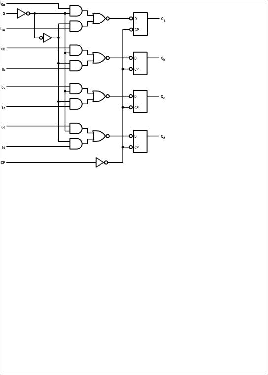
The 'AC/ACT399 is the logical equivalent of a quad 2-input multiplexer feeding into four edge-triggered flip-flops. A common Select input determines which of the two 4-bit words is accepted. The selected data enters the flip-flop on the rising edge of the clock.
Features
nICC reduced by 50%
nSelect inputs from two data sources
nFully positive edge-triggered operation
nOutputs source/sink 24 mA
nACT399 has TTL-compatible inputs
Logic Symbols |
Connection Diagrams |
Pin Assignment for DIP and Flatpak
DS100356-1
IEEE/IEC
DS100356-3
Pin Assignment
for LCC
|
DS100356-5 |
|
|
|
DS100356-2 |
|
|
|
Pin Names |
Description |
|
|
|
|
S |
Common Select Input |
|
CP |
Clock Pulse Input |
|
I0a±I 0d |
Data Inputs from Source 0 |
|
I1a±I1d |
Data Inputs from Source 1 |
|
Qa±Qd |
Register True Outputs |
|
TRI-STATE® is a registered trademark of National Semiconductor Corporation.
FACT® is a registered trademark of Fairchild Semiconductor Corporation.
Register Port-2 Quad 54ACT399
© 1998 National Semiconductor Corporation |
DS100356 |
www.national.com |

Functional Description
The 'AC/ACT399 is a high-speed quad 2-port register. It selects four bits of data from either of two sources (Ports) under control of a common Select input (S). The selected data is transferred to a 4-bit output register synchronous with the LOW-to-HIGH transition of the Clock input (CP). The 4-bit D-type output register is fully edge-triggered. The Data inputs (I0x, I1x) and Select input (S) must be stable only a setup time prior to and hold time after the LOW-to-HIGH transition of the Clock input for predictable operation.
Logic Diagram
Function Table
|
Inputs |
|
|
Outputs |
||
|
|
|
|
|
|
|
S |
I0 |
I1 |
CP |
Q |
|
|
Q |
||||||
L |
L |
X |
N |
L |
H |
|
L |
H |
X |
N |
H |
L |
|
H |
X |
L |
N |
L |
H |
|
H |
X |
H |
N |
H |
L |
|
H = HIGH Voltage Level
L = LOW Voltage Level
X = Immaterial
N = LOW-to-HIGH Clock Transition
DS100356-4
Please note that this diagram is provided only for the understanding of logic operations and should not be used to estimate propagation delays.
www.national.com |
2 |
 Loading...