


5962-8870401FA
54AC258•54ACT258
Quad 2-Input Multiplexer with TRI-STATE
®
Outputs
General Description
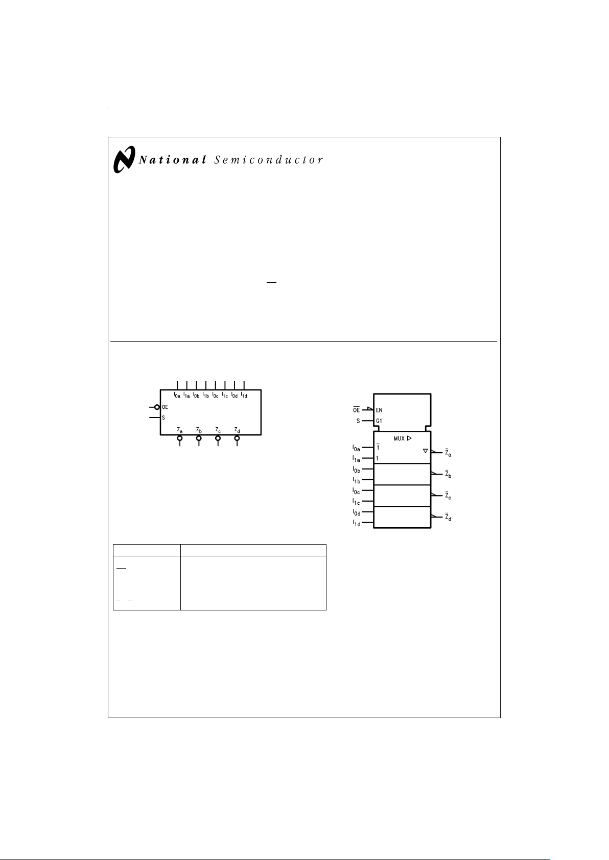
The ’AC/’ACT258 is a quad 2-input multiplexer with
TRI-STATE outputs. Four bits of data from two sources can
be selected usinga common data select input. The four outputs present the selected data in the complement (inverted)
form. The outputs may be switched to a high impedance
state with a HIGH on the common Output Enable (OE) input,
allowing the outputs to interface directly with bus-oriented
systems.
Features
n ICCand IOZreduced by 50
%
n Multiplexer expansion by tying outputs together
n Inverting TRI-STATE outputs
n Outputs source/sink 24 mA
n ’ACT258 has TTL-compatible inputs
n Standard Military Drawing (SMD)
—’ACT258: 5962-88704
—’AC258: 5962-91604
Logic Symbols
Pin Names Description
S Common Data Select Input
OE
TRI-STATE Output Enable Input
I
0a–I0d
Data Inputs from Source 0
I
1a–I1d
Data Inputs from Source 1
Z
a–Zd
TRI-STATE Inverting Data Outputs
TRI-STATE®is a registered trademark of National Semiconductor Corporation.
FACT
®
is a registered trademark of Fairchild Semiconductor Corporation.
DS100287-1
IEEE/IEC
DS100287-2
August 1998
54AC258
•
54ACT258 Quad 2-Input Multiplexer with TRI-STATE Outputs
© 1998 National Semiconductor Corporation DS100287 www.national.com
Connection Diagrams Functional Description
The ’AC/’ACT258 is a quad 2-input multiplexer with
TRI-STATE outputs. It selects four bits of data from two
sources under control of a common Select input (S). When
the Select inputis LOW, the I
0x
inputs are selectedand when
Select is HIGH, the I
1x
inputs are selected. The data on the
selected inputs appears at the outputs in inverted form. The
’AC/’ACT258 is the logic implementation of a 4-pole,
2-position switch where the position of the switch is determined by the logic levels supplied to the Select input. The
logic equations for the outputs are shown below:
Z
a
=
OE
•
(I
1a
•
S+I
0a
•
S)
Z
b
=
OE
•
(I
1b
•
S+I
0b
•
S)
Z
c
=
OE
•
(I
1c
•
S+I
0c
•
S)
Z
d
=
OE
•
(I
1d
•
S+I
0d
•
S)
When the Output Enable input (OE) is HIGH, the outputs are
forced to a high impedance state. If the outputs of the
TRI-STATE devices are tied together, all but one device must
be in the high impedance state to avoid high currents that
would exceed the maximum ratings. Designers should ensure that Output Enable signals to TRI-STATE devices
whose outputs are tied together are designed so there is no
overlap.
Truth Table
Output Select Data Outputs
Enable Input Inputs
OE
SI
0
I
1
Z
HXXXZ
LHXLH
LHXHL
LLLXH
LLHXL
H
=
HIGH Voltage Level
L=LOW Voltage Level
X=Immaterial
Z=High Impedance
Pin Assignment
for DIP and Flatpak
DS100287-3
Pin Assignment
for LCC
DS100287-4
www.national.com 2
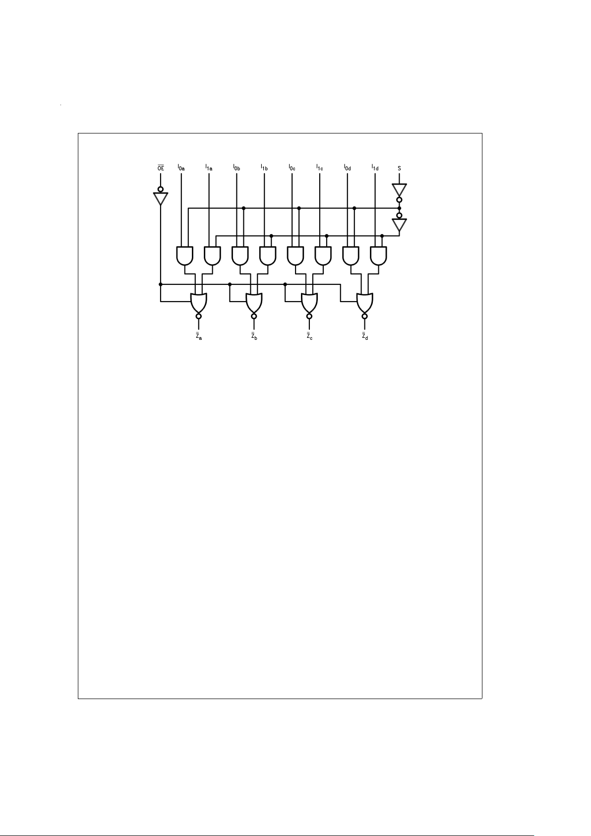
Logic Diagram
DS100287-5
Please note that this diagram is provided only for the understanding of logic operations and should not be used to estimate propagation delays.
www.national.com3
 Loading...