


54F373LMQB
TL/F/9523
54F/74F373 Octal Transparent Latch with TRI-STATE Outputs
May 1995
54F/74F373
Octal Transparent Latch with TRI-STATE
É
Outputs
General Description
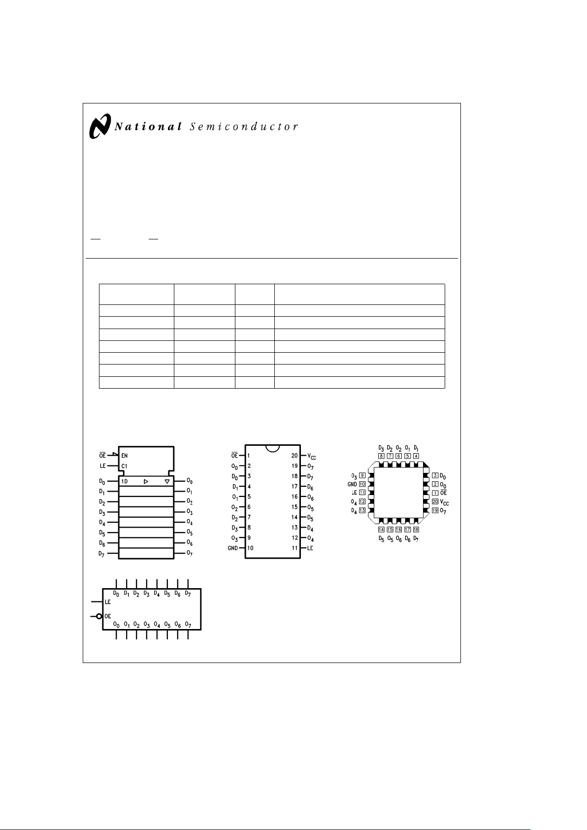
The ’F373 consists of eight latches with TRI-STATE outputs
for bus organized system applications. The flip-flops appear
transparent to the data when Latch Enable (LE) is HIGH.
When LE is LOW, the data that meets the setup times is
latched. Data appears on the bus when the Output Enable
(OE
) is LOW. When OE is HIGH the bus output is in the high
impedance state.
Features
Y
Eight latches in a single package
Y
TRI-STATE outputs for bus interfacing
Y
Guaranteed 4000V minimum ESD protection
Commercial Military
Package
Package Description
Number
74F373PC N20A 20-Lead (0.300
×
Wide) Molded Dual-In-Line
54F373DM (QB) J20A 20-Lead Ceramic Dual-In-Line
74F373SC (Note 1) M20B 20-Lead (0.300
×
Wide) Molded Small Outline, JEDEC
74F373SJ (Note 1) M20D 20-Lead (0.300
×
Wide) Molded Small Outline, EIAJ
74F373MSA (Note 1) MSA20 20-Lead Molded Shrink Small Outline, EIAJ Type II
54F373FM (QB) W20A 20-Lead Cerpack
54F373LM (QB) E20A 20-Lead Ceramic Leadless Chip Carrier, Type C
Note 1: Devices also available in 13
×
reel. Use suffix
e
SCX, SJX, and MSAX.
Logic Symbols Connection Diagrams
IEEE/IEC
TL/F/9523– 4
TL/F/9523– 1
Pin Assignment
for DIP, SOIC, SSOP and Flatpak
TL/F/9523– 2
Pin Assignment
for LCC
TL/F/9523– 3
TRI-STATE
É
is a registered trademark of National Semiconductor Corporation.
C
1995 National Semiconductor Corporation RRD-B30M75/Printed in U. S. A.
Unit Loading/Fan Out
54F/74F
Pin Names Description
U.L. Input I
IH
/I
IL
HIGH/LOW Output I
OH
/I
OL
D
0
–D
7
Data Inputs 1.0/1.0 20 mA/
b
0.6 mA
LE Latch Enable Input (Active HIGH) 1.0/1.0 20 mA/
b
0.6 mA
OE
Output Enable Input (Active LOW) 1.0/1.0 20 m A/
b
0.6 mA
O
0
–O
7
TRI-STATE Latch Outputs 150/40 (33.3)
b
3 mA/24 mA (20 mA)
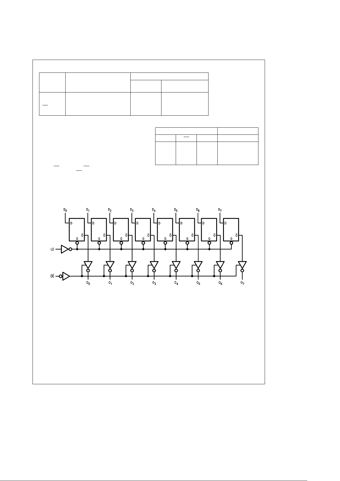
Functional Description
The ’F373 contains eight D-type latches with TRI-STATE
output buffers. When the Latch Enable (LE) input is HIGH,
data on the D
n
inputs enters the latches. In this condition
the latches are transparent, i.e., a latch output will change
state each time its D input changes. When LE is LOW, the
latches store the information that was present on the D in-
puts a setup time preceding the HIGH-to-LOW transition of
LE. The TRI-STATE buffers are controlled by the Output
Enable (OE
) input. When OE is LOW, the buffers are in the
bi-state mode. When OE
is HIGH the buffers are in the high
impedance mode but this does not interfere with entering
new data into the latches.
Truth Table
Inputs Output
LE OE D
n
O
n
HLH H
HLL L
LLXO
n
(no change)
XHX Z
H
e
HIGH Voltage Level
L
e
LOW Voltage Level
X
e
Immaterial
Z
e
High Impedance State
Logic Diagram
TL/F/9523– 5
Please note that this diagram is provided only for the understanding of logic operations and should not be used to estimate propagation delays.
2
Absolute Maximum Ratings (Note 1)
If Military/Aerospace specified devices are required,
please contact the National Semiconductor Sales
Office/Distributors for availability and specifications.
Storage Temperature
b
65
§
Cto
a
150
§
C
Ambient Temperature under Bias
b
55
§
Cto
a
125
§
C
Junction Temperature under Bias
b
55
§
Cto
a
175
§
C
Plastic
b
55
§
Cto
a
150
§
C
V
CC
Pin Potential to
Ground Pin
b
0.5V to
a
7.0V
Input Voltage (Note 2)
b
0.5V to
a
7.0V
Input Current (Note 2)
b
30 mA to
a
5.0 mA
Note 1: Absolute maximum ratings are values beyond which the device may
be damaged or have its useful life impaired. Functional operation under
these conditions is not implied.
Note 2: Either voltage limit or current limit is sufficient to protect inputs.
Voltage Applied to Output
in HIGH State (with V
CC
e
0V)
Standard Output
b
0.5V to V
CC
TRI-STATE Output
b
0.5V to
a
5.5V
Current Applied to Output
in LOW State (Max) twice the rated I
OL
(mA)
ESD Last Passing Voltage (Min) 4000V
Recommended Operating
Conditions
Free Air Ambient Temperature
Military
b
55
§
Cto
a
125
§
C
Commercial 0
§
Cto
a
70
§
C
Supply Voltage
Military
a
4.5V to
a
5.5V
Commercial
a
4.5V to
a
5.5V
DC Electrical Characteristics
Symbol Parameter
54F/74F
Units V
CC
Conditions
Min Typ Max
V
IH
Input HIGH Voltage 2.0 V Recognized as a HIGH Signal
V
IL
Input LOW Voltage 0.8 V Recognized as a LOW Signal
V
CD
Input Clamp Diode Voltage
b
1.2 V Min I
IN
eb
18 mA
V
OH
Output HIGH 54F 10% V
CC
2.5 I
OH
eb
1mA
Voltage 54F 10% V
CC
2.4 I
OH
eb
3mA
74F 10% V
CC
2.5
V Min
I
OH
eb
1mA
74F 10% V
CC
2.4 I
OH
eb
3mA
74F 5% V
CC
2.7 I
OH
eb
1mA
74F 5% V
CC
2.7 I
OH
eb
3mA
V
OL
Output LOW 54F 10% V
CC
0.5
V Min
I
OL
e
20 mA
Voltage 74F 10% V
CC
0.5 I
OL
e
24 mA
I
IH
Input HIGH Current 54F 20.0
mA Max V
IN
e
2.7V
74F 5.0
I
BVI
Input HIGH Current 54F 100
mA Max V
IN
e
7.0V
Breakdown Test 74F 7.0
I
CEX
Output HIGH 54F 250
mA Max V
OUT
e
V
CC
Leakage Current 74F 50
V
ID
Input Leakage
74F 4.75 V 0.0
I
ID
e
1.9 mA
Test All Other Pins Grounded
I
OD
Output Leakage
74F 3.75 mA 0.0
V
IOD
e
150 mV
Circuit Current All Other Pins Grounded
I
IL
Input LOW Current
b
0.6 mA Max V
IN
e
0.5V
I
OZH
Output Leakage Current 50 mA Max V
OUT
e
2.7V
I
OZL
Output Leakage Current
b
50 mA Max V
OUT
e
0.5V
I
OS
Output Short-Circuit Current
b
60
b
150 mA Max V
OUT
e
0V
I
ZZ
Bus Drainage Test 500 mA 0.0V V
OUT
e
5.25V
I
CCZ
Power Supply Current 38 55 mA Max V
O
e
HIGH Z
3
 Loading...