


NSC ADC08832IN, ADC08832IMX, ADC08832IMMX, ADC08832IMM, ADC08832IM Datasheet
...September 1999
ADC08831/ADC08832
8-Bit Serial I/O CMOS A/D Converters with Multiplexer
and Sample/Hold Function
General Description
The ADC08831/ADC08832 are 8-bit successive approximation Analog to Digital converters with 3-wire serial interfaces and a configurable input multiplexer for 2 channels. The serial I/O will interface to COPS™ family of micro-controllers, PLD's, microprocessors, DSP's, or shift registers. The serial I/O is configured to comply with the NSC MICROWIRE™ serial data exchange standard.
To minimize total power consumption, the ADC08831/ADC08832 automatically go into low power mode whenever they are not performing conversions.
A track/hold function allows the analog voltage at the positive input to vary during the actual A/D conversion.
The analog inputs can be configured to operate in various combinations of single-ended, differential, or pseudo-differential modes. The voltage reference input can be adjusted to allow encoding of small analog voltage spans to the full 8-bits of resolution.
Applications
nDigitizing sensors and waveforms
nProcess control monitoring
nRemote sensing in noisy environments
nInstrumentation
nEmbedded Systems
Features
n3-wire serial digital data link requires few I/O pins
nAnalog input track/hold function
n2-channel input multiplexer option with address logic
nAnalog input voltage range from GND to VCC
nNo zero or full scale adjustment required
nTTL/CMOS input/output compatible
nSuperior pin compatible replacement for ADC0831/2
Key Specifications
nResolution: 8 bits
nConversion time (fC = 2 MHz): 4µs (max)
nPower dissipation: 8.5mW (typ)
nLow power mode: 3.0mW (typ)
nSingle supply: 5VDC
nTotal unadjusted error: ±1LSB
nNo missing codes over temperature
Typical Application
DS100108-44
DS100108-43
COPS™ is a trademark of National Semiconductor Corporation.
MICROWIRE™ is a trademark of National Semiconductor Corporation.
TRI-STATE™
Sample/Hold and Multiplexer with Converters A/D CMOS I/O Serial Bit-8 ADC08831/ADC08832
Function
© 1999 National Semiconductor Corporation |
DS100108 |
www.national.com |
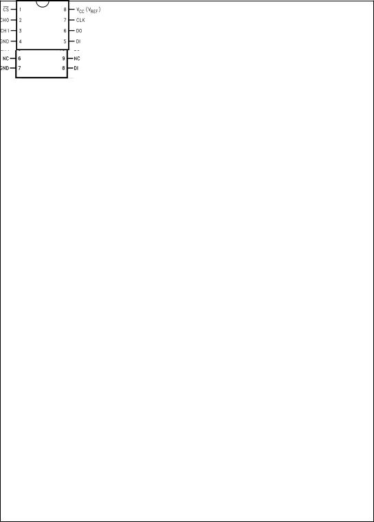
Connection Diagrams
ADC08831 |
ADC08832 |
Wide Body SO Packages |
Wide Body SO Packages |
DS100108-4 |
DS100108-3 |
ADC08831 |
ADC08832 |
N,M,MM Packages |
N,M,MM Packages |
DS100108-2 DS100108-1
Ordering Information
Temperature Range |
Package |
|
|
|
|
Industrial (−40ÊC ≤ TJ ≤ +85ÊC) |
|
|
ADC08831IN |
N08E |
|
|
||
ADC08832IN |
||
|
||
|
|
|
ADC08831IWM, |
M14B |
|
|
||
ADC08832IWM, |
||
|
||
|
|
|
ADC08831IM, |
M08A |
|
|
||
ADC08832IM, |
||
|
||
|
|
|
ADC08831IMM, |
MUA08A |
|
|
||
ADC08832IMM, |
||
|
||
|
|
www.national.com |
2 |

Absolute Maximum Ratings (Notes 1, 3)
If Military/Aerospace specified devices are required, please contact the National Semiconductor Sales Office/ Distributors for availability and specifications.
Supply Voltage (VCC) |
6.5V |
Voltage at Inputs and Outputs |
−0.3V to V CC + 0.3V |
Input Current at Any Pin (Note 4) |
±5 mA |
Package Input Current (Note 4) |
±20 mA |
ESD Susceptibility (Note 6) |
|
Human Body Model |
2000V |
Machine Model |
200V |
Junction Temperature (Note 5) |
150ÊC |
Storage Temperature Range |
−65Ê C to 150ÊC |
Mounting Temperature |
|
Lead Temp. (soldering, 10 sec) |
260ÊC |
Infrared (10 sec) |
215ÊC |
Operating Ratings(Notes 2, 3)
Temperature Range |
−40ÊC ≤ TJ ≤ +85ÊC |
Supply Voltage |
4.5 V to 6.0 V |
Thermal Resistance (θjA) |
|
SO Package, 8-pin Surface Mount |
190ÊC/W |
MSOP, 8-pin Surface Mount |
235ÊC/W |
SO Package, 14-pin Surface Mount |
145ÊC/W |
N Package, 8-pin |
122ÊC/W |
Clock Frequency |
10kHz≤fCLK≤2MHz |
Electrical Characteristics
The following specifications apply for VCC = VREF = +5VDC, and fCLK = 2 MHz unless otherwise specified. Boldface limits apply for TA = TJ = TMIN to TMAX; all other limits TA = TJ = 25ÊC.
Symbol |
Parameter |
|
Conditions |
Typical |
Limits |
|
Units |
|||
|
|
|
|
|
|
|
(Note 8) |
(Note 9) |
|
(Limits) |
|
|
|
|
|
|
|
|
|
||
CONVERTER AND MULTIPLEXER CHARACTERISTICS |
|
|
|
|
|
|
||||
|
|
|
|
|
|
|
|
|||
TUE |
Total Unadjusted Error |
|
(Note 10) |
±0.3 |
± |
1 |
LSB |
|||
|
|
|
|
|
|
|
|
|
|
(max) |
|
Offset Error |
|
|
|
|
|
±0.2 |
|
|
LSB |
|
|
|
|
|
|
|
|
|
|
|
DNL |
Differential NonLinearity |
|
|
|
|
|
±0.2 |
|
|
LSB |
|
|
|
|
|
|
|
|
|
|
|
INL |
Integral NonLinearity |
|
|
|
|
|
±0.2 |
|
|
LSB |
|
|
|
|
|
|
|
|
|
|
|
FS |
Full Scale Error |
|
|
|
|
|
±0.3 |
|
|
LSB |
RREF |
Reference Input Resistance |
|
(Note 11) |
3.5 |
2.8 |
kΩ (min) |
||||
|
|
|
|
|
|
|
|
5.9 |
kΩ (max) |
|
|
|
|
|
|
|
|
||||
VIN |
Analog Input Voltage |
|
(Note 12) |
|
(VCC + 0.05) |
V (max) |
||||
|
|
|
|
|
|
|
|
(GND − 0.05) |
V (min) |
|
|
|
|
|
|
|
|
|
|
|
|
|
DC Common-Mode Error |
|
|
|
|
|
|
± |
1¤4 |
LSB (max) |
|
Power Supply Sensitivity |
VCC |
= |
|
± |
10%, |
|
± |
1 4 |
|
|
|
5V |
|
|
± |
¤ |
LSB (max) |
|||
|
|
VCC = 5V ±5% |
|
1¤4 |
LSB (max) |
|||||
|
On Channel Leakage Current |
On Channel = 5V, |
|
0.2 |
µA (max) |
|||||
|
(Note 13) |
Off Channel = 0V |
|
1 |
|
|||||
|
|
|
|
|
|
|||||
|
|
On Channel = 0V |
|
−0.2 |
µA (min) |
|||||
|
|
Off Channel = 5V |
|
−1 |
|
|||||
|
|
|
|
|
|
|||||
|
Off Channel Leakage Current |
On Channel = 5V, |
|
−0.2 |
µA (min) |
|||||
|
(Note 13) |
Off Channel = 0V |
|
−1 |
|
|||||
|
|
|
|
|
|
|||||
|
|
On Channel = 0V, |
|
0.2 |
µA (max) |
|||||
|
|
Off Channel = 5V |
|
1 |
|
|||||
|
|
|
|
|
|
|
|
|
|
|
DC CHARACTERISTICS |
|
|
|
|
|
|
|
|
|
|
|
|
|
|
|
|
|
|
|
|
|
VIN(1) |
Logical ª1º Input Voltage |
|
|
|
|
|
|
2.0 |
V (min) |
|
VIN(0) |
Logical ª0º Input Voltage |
|
|
|
|
|
|
0.8 |
V (max) |
|
IIN(1) |
Logical ª1º Input Current |
VIN = 5.0V |
|
0.05 |
+1 |
µA (max) |
||||
IIN(0) |
Logical ª0º Input Current |
VIN = 0V |
|
|
0.05 |
−1 |
µA (max) |
|||
VOUT(1) |
Logical ª1º Output Voltage |
VCC = 4.75V: |
|
|
|
|
||||
|
|
IOUT = −360 µA |
|
2.4 |
V (min) |
|||||
|
|
IOUT = −10 µA |
|
4.5 |
V (min) |
|||||
VOUT(0) |
Logical ª0º Output Voltage |
VCC = 4.75V |
|
0.4 |
V (max) |
|||||
|
|
IOUT = 1.6 mA |
|
|
|
|
||||
IOUT |
TRI-STATE Output Current |
VOUT = 0V |
|
|
−3.0 |
µA (max) |
||||
|
|
VOUT = 5V |
|
|
3.0 |
µA (max) |
||||
ISOURCE |
Output Source Current |
VOUT = 0V |
|
|
−6.5 |
mA (max) |
||||
ISINK |
Output Sink Current |
VOUT = VCC |
|
8.0 |
mA (min) |
|||||
3 |
www.national.com |

Electrical Characteristics (Continued)
The following specifications apply for VCC = VREF = +5VDC, and fCLK = 2 MHz unless otherwise specified. Boldface limits apply for TA = TJ = TMIN to TMAX; all other limits TA = TJ = 25ÊC.
Symbol |
Parameter |
|
|
Conditions |
Typical |
Limits |
Units |
|
|
|
|
|
|
|
(Note 8) |
(Note 9) |
(Limits) |
DC CHARACTERISTICS |
|
|
|
|
|
|
|
|
|
|
|
|
|
|
|
|
|
ICC |
Supply Current |
ADC08831 |
|
CS |
= VCC |
0.6 |
1.0 |
mA (max) |
|
CLK = VCC |
|
|
|
|
|
|
|
|
|
|
|
= LOW |
1.7 |
2.4 |
mA (max) |
|
|
|
CS |
||||||
ICC |
Supply Current |
ADC08832 |
|
|
= VCC |
1.3 |
1.8 |
mA (max) |
|
CS |
|||||||
|
CLK = VCC (Note 16) |
|
|
= LOW |
2.4 |
3.5 |
mA (max) |
|
|
CS |
|||||||
Electrical Characteristics
The following specifications apply for VCC = VREF = +5 VDC, and tr = tf = 20 ns unless otherwise specified. Boldface limits apply for TA = TJ = TMIN to TMAX; all other limits TA = TJ = 25ÊC.
Symbol |
|
|
|
|
Parameter |
Conditions |
Typical |
Limits |
Units |
|
|
|
|
|
|
|
(Note 8) |
(Note 9) |
(Limits) |
|
|
|
|
|
|
|
|
|
|
fCLK |
|
Clock Frequency |
|
|
2 |
MHz (max) |
|||
|
Clock Duty Cycle |
|
|
40 |
% (min) |
||||
|
(Note 14) |
|
|
60 |
% (max) |
||||
TC |
|
Conversion Time (Not Including MUX |
fCLK = 2MHz |
|
8 |
1/fCLK (max) |
|||
|
|
Addressing Time) |
|
|
4 |
µs (max) |
|||
|
|
|
|
|
|
|
|
|
|
tCA |
|
Acquisition Time |
|
|
1¤2 |
1/fCLK (max) |
|||
tSET-UP |
|
|
|
|
|
|
25 |
ns (min) |
|
|
CS |
Falling Edge or Data Input |
|
|
|||||
|
|
Valid to CLK Rising Edge |
|
|
|
|
|||
|
|
|
|
|
|
|
|
|
|
tHOLD |
|
Data Input Valid after CLK |
|
|
20 |
ns (min) |
|||
|
|
Rising Edge |
|
|
|
|
|||
|
|
|
|
|
|
|
|
|
|
tpd1, tpd0 |
|
CLK Falling Edge to Output |
CL = 100 pF: |
|
|
|
|||
|
|
Data Valid (Note 15) |
Data MSB First |
|
250 |
ns (max) |
|||
|
|
|
|
|
|
Data LSB First |
|
200 |
ns (max) |
|
|
|
|
|
|
|
|
|
|
t1H, t0H |
|
TRI-STATE Delay from Rising Edge |
CL = 10 pF, RL = 10 kΩ |
50 |
|
ns |
|||
|
|
of |
CS |
to Data Output and SARS Hi-Z |
(see TRI-STATE Test Circuits) |
|
|
|
|
|
|
|
|
|
|
CL = 100 pF, RL = 2 kΩ |
|
180 |
ns (max) |
CIN |
|
Capacitance of Analog Input (Note 17) |
|
13 |
|
pF |
|||
CIN |
|
Capacitance of Logic Inputs |
|
5 |
|
pF |
|||
COUT |
|
Capacitance of Logic Outputs |
|
5 |
|
pF |
|||
www.national.com |
4 |

Dynamic Characteristics
The following specifications apply for VCC = 5V, fCLK = 2MHz, TA= 25ÊC, RSOURCE = 50Ω, fIN = 45kHz, VIN = 5VP, VREF = 5V, non-coherent 2048 samples with windowing.
Symbol |
Parameter |
Conditions |
Typical |
Limits |
Units |
|
|
|
(Note 8) |
(Note 9) |
(Limits) |
|
|
|
|
|
|
fS |
Sampling Rate ADC08831 |
fCLK/11 |
|
181 |
ksps |
|
ADC08832 |
fCLK/13 (Note 21) |
|
153 |
ksps |
SNR |
Signal-to -Noise Ratio (Note 19) |
|
48.5 |
|
dB |
|
|
|
|
|
|
THD |
Total Harmonic Distortion (Note 20) |
|
−59.5 |
|
dB |
|
|
|
|
|
|
SINAD |
Signal-to -Noise and Distortion |
|
48.0 |
|
dB |
|
|
|
|
|
|
ENOB |
Effective Number Of Bits (Note 18) |
|
7.7 |
|
Bits |
|
|
|
|
|
|
SFDR |
Spurious Free Dynamic Range |
|
62.5 |
|
dB |
|
|
|
|
|
|
Note 1: Absolute Maximum Ratings indicate limits beyond which damage to the device may occur.
Note 2: Operating Ratings indicate conditions for which the device is functional. These ratings do not guarantee specific performance limits. For guaranteed specifications and test conditions, see the Electrical Characteristics. The guaranteed specifications apply only for the test conditions listed. Some performance characteristics may degrade when the device is not operated under the listed test conditions.
Note 3: All voltages are measured with respect to GND = 0 VDC, unless otherwise specified.
Note 4: When the input voltage VIN at any pin exceeds the power supplies (VIN < (GND) or VIN > VCC,) the current at that pin should be limited to 5 mA. The 20 mA maximum package input current rating limits the number of pins that can safely exceed the power supplies with an input current of 5 mA to four pins.
Note 5: The maximum power dissipation must be derated at elevated temperatures and is dictated by TJMAX, qJA and the ambient temperature, TA. The maximum allowable power dissipation at any temperature is PD = (TJMAX − T A)/qJA or the number given in the Absolute Maximum Ratings, whichever is lower.
Note 6: Human body model, 100 pF capacitor discharged through a 1.5 kW resistor. The machine mode is a 200pF capacitor discharged directly into each pin.
Note 7: See AN450 ªSurface Mounting Methods and Their Effect on Product Reliabilityº or Linear Data Book section ªSurface Mountº for other methods of soldering surface mount devices.
Note 8: Typicals are at TJ = 25ÊC and represent the most likely parametric norm.
Note 9: Guaranteed to National's AOQL (Average Outgoing Quality Level).
Note 10: Total Unadjusted Error (TUE) includes offset, full-scale, linearity, multiplexer errors.
Note 11: It is not tested for the ADC08832.
Note 12: For VIN(−) ³ VIN(+) the digital code will be 0000 0000. Two on-chip diodes are tied to each analog input (see Functional Block Diagram) which will forward-conduct for analog input voltages one diode drop below ground or one diode drop greater than VCC supply. During testing at low VCC levels (e.g., 4.5V), high
level analog inputs (e.g., 5V) can cause an input diode to conduct, especially at elevated temperatures, which will cause errors for analog inputs near full-scale. The spec allows 50 mV forward bias of either diode; this means that as long as the analog VIN does not exceed the supply voltage by more than 50 mV, the output code will be correct. Exceeding this range on an unselected channel will corrupt the reading of a selected channel. Achievement of an absolute 0 VDC to 5 VDC input voltage range will therefore require a minimum supply voltage of 4.950 VDC over temperature variations, initial tolerance and loading.
Note 13: Channel leakage current is measured after a single-ended channel is selected and the clock is turned off. For off channel leakage current the following two cases are considered: one, with the selected channel tied high (5 VDC) and the remaining off channel tied low (0 VDC), total current flow through the off channel is measured; two, with the selected channel tied low and the off channels tied high, total current flow through the off channel is again measured. The two cases considered for determining on channel leakage current are the same except total current flow through the selected channel is measured.
Note 14: A 40% to 60% duty cycle range insures proper operation at all clock frequencies. In the case that an available clock has a duty cycle outside of these limits the minimum time the clock is high or low must be at least 250 ns. The maximum time the clock can be high or low is 60 µs.
Note 15: Since data, MSB first, is the output of the comparator used in the successive approximation loop, an additional delay is built in to allow for comparator response time.
Note 16: For the ADC08832 Vref is internally tied to VCC, therefore, for the ADC08832 reference current is included in the supply current.
Note 17: Analog inputs are typically 300 ohms input resistance to a 13pF sample and hold capacitor.
Note 18: Effective Number Of Bits (ENOB) is calculated from the measured signal-to-noise plus distortion ratio (SINAD) using the equation ENOB = (SINAD-1.76)/ 6.02.
Note 19: The signal-to-noise ratio is the ratio of the signal amplitude to the background noise level. Harmonics of the input signal are not included in it's calculation.
Note 20: The contributions from the first 6 harmonics are used in the calculation of the THD.
Note 21: The maximum sampling rate is slightly less than fCLK/11 if CS is reset in less than one clock period.
5 |
www.national.com |

Block Diagram
DS100108-47
*For ADC08831 VREF pin is available, for ADC08832 DI pin is available, and VREF is tied to VCC Pin names in parentheses refer to ADC08832
www.national.com |
6 |
Typical Performance Characteristics The following specifications apply for TA = 25ÊC, VCC = VREF = 5V, unless otherwise specified.
Linearity Error (TUE) vs |
Linearity Error (TUE) vs |
Linearity Error (TUE) vs |
Reference Voltage |
Temperature |
Clock Frequency |
DS100108-27 DS100108-15
Power Supply Current vs |
Power Supply Current vs |
Temperature (ADC08831) |
Temperature (ADC08832) |
DS100108-14
Power Supply Current
vs Clock Frequency, CS = Low, ADC08831
DS100108-35 |
DS100108-36 |
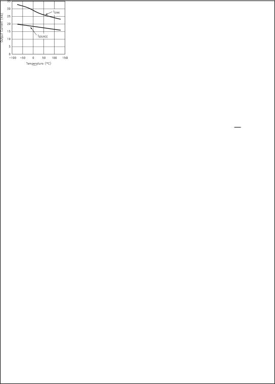
DS100108-37
Output Current vs
Temperature
DS100108-33
7 |
www.national.com |
 Loading...