


NSC 5962R9218701VSA, 5962R9218701VRA, 5962R9218701V2A, 5962R9218701MSA, 5962R9218701MRA Datasheet
...
September 1998
54ACQ245 · 54ACTQ245
Quiet Series Octal Bidirectional Transceiver with TRI-STATE® Inputs/Outputs
General Description
The 'ACQ/'ACTQ245 contains eight non-inverting bidirectional buffers with TRI-STATE outputs and is intended for bus-oriented applications. Current sinking capability is 24 mA at both the A and B ports. The Transmit/Receive (T/R) input determines the direction of data flow through the bidirectional transceiver. Transmit (active-HIGH) enables data from A ports to B ports; Receive (active-LOW) enables data from B ports to A ports. The Output Enable input, when HIGH, disables both A and B ports by placing them in a HIGH Z condition.
The 'ACQ/'ACTQ utilizes NSC Quiet Series technology to guarantee quiet output switching and improve dynamic threshold performance. FACT Quiet Series™ features GTO™ output control and undershoot corrector in addition to a split ground bus for superior performance.
Features
nICC and IOZ reduced by 50%
nGuaranteed simultaneous switching noise level and dynamic threshold performance
nImproved latch-up immunity
nTRI-STATE outputs drive bus lines or buffer memory address registers
nOutputs source/sink 24 mA
nFaster prop delays than the standard 'ACT245
n4 kV minimum ESD immunity ('ACQ)
nStandard Military Drawing (SMD)
Ð'ACTQ245: 5962-92187
Ð'ACQ245: 5962-92177
Logic Symbols
IEEE/IEC
DS100237-1
DS100237-2
|
|
|
|
Pin |
Description |
|
|
Names |
|
||
|
|
|
|
|
|
|
|
|
|
Output Enable Input |
|
|
OE |
|
|
||
|
|
|
Transmit/Receive Input |
||
T/R |
|
||||
A0±A7 |
Side A TRI-STATE Inputs or TRI-STATE Outputs |
||||
B0±B7 |
Side B TRI-STATE Inputs or TRI-STATE Outputs |
||||
GTO™ is a trademark of National Semiconductor Corporation.
TRI-STATE® is a registered trademark of National Semiconductor Corporation.
FACT® is a registered trademark of Fairchild Semiconductor Corporation.
FACT Quiet Series™ is a trademark of Fairchild Semiconductor Corporation.
STATE-TRI with Transceiver Bidirectional Octal Series Quiet 54ACTQ245 · 54ACQ245 Inputs/Outputs
© 1998 National Semiconductor Corporation |
DS100237 |
www.national.com |
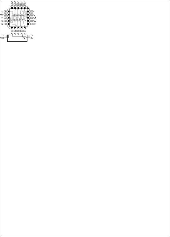
Connection Diagrams
Pin Assignment for |
Pin Assignment |
DIP and Flatpak |
for LCC |
DS100237-4
|
|
|
|
|
|
DS100237-3 |
Truth Table |
||||||
|
|
|
|
|
|
|
|
Inputs |
Outputs |
||||
|
|
|
|
|
|
|
|
OE |
|
T/R |
|
|
|
|
L |
L |
Bus B Data to Bus A |
|||
|
L |
H |
Bus A Data to Bus B |
|||
|
H |
X |
HIGH-Z State |
|||
|
|
|
|
|
|
|
H = HIGH Voltage Level
L = LOW Voltage Level
X = Immaterial
www.national.com |
2 |

Absolute Maximum Ratings (Note 1)
If Military/Aerospace specified devices are required, please contact the National Semiconductor Sales Office/ Distributors for availability and specifications.
Supply Voltage (VCC) |
−0.5V to +7.0V |
DC Input Diode Current (IIK) |
|
VI = −0.5V |
−20 mA |
VI = VCC + 0.5V |
+20 mA |
DC Input Voltage (VI) |
−0.5V to V CC + 0.5V |
DC Output Diode Current (IOK) |
|
VO = −0.5V |
−20 mA |
VO = VCC + 0.5V |
+20 mA |
DC Output Voltage (VO) |
−0.5V to V CC + 0.5V |
DC Output Source |
|
or Sink Current (IO) |
±50 mA |
DC VCC or Ground Current |
|
per Output Pin (ICC or IGND) |
±50 mA |
Storage Temperature (TSTG) |
−65ÊC to +150ÊC |
DC Latch-Up Source or |
|
Sink Current |
±300 mA |
Junction Temperature (TJ) |
|
CDIP |
175ÊC |
Recommended Operating
Conditions
Supply Voltage (VCC) |
|
|
'ACQ |
|
2.0V to 6.0V |
'ACTQ |
|
4.5V to 5.5V |
Input Voltage (VI) |
|
0V to VCC |
Output Voltage (VO) |
|
0V to VCC |
Operating Temperature (TA) |
|
|
54ACQ/ACTQ |
|
−55ÊC to +125ÊC |
Minimum Input Edge Rate |
V/ |
t |
'ACQ Devices |
|
|
VIN from 30% to 70% of VCC |
|
|
VCC @ 3.0V, 4.5V, 5.5V |
|
125 mV/ ns |
Minimum Input Edge Rate |
V/ |
t |
'ACTQ Devices |
|
|
VIN from 0.8V to 2.0V |
|
|
VCC @ 4.5V, 5.5V |
|
125 mV/ns |
Note 1: Absolute maximum ratings are those values beyond which damage to the device may occur. The databook specifications should be met, without exception, to ensure that the system design is reliable over its power supply, temperature, and output/input loading variables. National does not recommend operation of FACT® circuits outside databook specifications.
DC Characteristics for 'ACQ Family Devices
|
|
|
54ACQ |
|
|
|
|
|
|
|
|
|
|
Symbol |
Parameter |
VCC |
TA = |
Units |
Conditions |
|
|
|
(V) |
−55ÊC to +125ÊC |
|
|
|
|
|
|
|
|
|
|
|
|
|
Guaranteed Limits |
|
|
|
|
|
|
|
|
|
|
VIH |
Minimum High |
3.0 |
2.1 |
|
VOUT = 0.1V |
|
|
Level Input |
4.5 |
3.15 |
V |
or VCC − 0.1V |
|
|
Voltage |
5.5 |
3.85 |
|
|
|
|
|
|
|
|
|
|
VIL |
Maximum Low |
3.0 |
0.9 |
|
VOUT = 0.1V |
|
|
Level Input |
4.5 |
1.35 |
V |
or VCC − 0.1V |
|
|
Voltage |
5.5 |
1.65 |
|
|
|
|
|
|
|
|
|
|
VOH |
Minimum High |
3.0 |
2.9 |
|
IOUT = −50 µA |
|
|
Level Output |
4.5 |
4.4 |
V |
|
|
|
Voltage |
5.5 |
5.4 |
|
|
|
|
|
|
|
|
|
|
|
|
|
|
|
(Note 2) |
|
|
|
|
|
|
VIN = VIL or VIH |
|
|
|
3.0 |
2.4 |
|
|
−12 mA |
|
|
4.5 |
3.7 |
V |
IOH |
−24 mA |
|
|
5.5 |
4.7 |
|
|
−24 mA |
|
|
|
|
|
|
|
VOL |
Maximum Low |
3.0 |
0.1 |
|
IOUT = 50 µA |
|
|
Level Output |
4.5 |
0.1 |
V |
|
|
|
Voltage |
5.5 |
0.1 |
|
|
|
|
|
|
|
|
(Note 2) |
|
|
|
|
|
|
VIN = VIL or VIH |
|
|
|
3.0 |
0.50 |
|
|
12 mA |
|
|
4.5 |
0.50 |
V |
IOL |
24 mA |
|
|
5.5 |
0.50 |
|
|
24 mA |
IIN |
Maximum Input |
5.5 |
±1.0 |
µA |
VI = VCC, GND |
|
|
Leakage Current |
|
|
|
(Note 4) |
|
|
|
|
|
|
|
|
3 |
www.national.com |
 Loading...