


CD4015BCN
October 1987
Revised January 1999
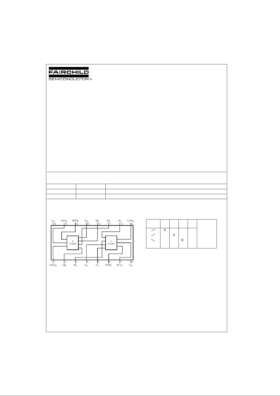
CD4015BC Dual 4-Bit Static Shift Register
© 1999 Fairchild Semiconductor Corporation DS005948.prf www.fairchildsemi.com
CD4015BC
Dual 4-Bit Static Shift Register
General Description
The CD4015BC contains two identical, 4-stage, serial-
input/parallel-output registers with independent “Data”,
“Clock,” and “Reset” inputs. Th e logic level present at the
input of each stage is transferred to the output of that stage
at each positive-going clock transition. A logi c high on the
“Reset” input resets al l four stages covered by that input.
All inputs are protected from static discharge by a series
resistor and diode clamps to V
DD
and V
SS
.
Features
■ Wide supply voltage range: 3.0V to 18V
■ High noise immunity: 0.45 V
DD
(typ.)
■ Low power TTL: Fan out of 2 driving 74L
compatibility: or 1 driving 74LS
■ Medium speed operation: 8 MHz (typ.) clock rate
■ Fully static design: @V
DD
− V
SS
= 10V
Applications
• Serial-input/parallel-output data queueing
• Serial to parallel data conversion
• General purpose register
Ordering Code:
Devices also available in Tape and Reel. Specify by appending the suffix letter “X” to the ordering code.
Connection Diagram
Pin Assignments for DIP and SOIC
Truth Table
X = Don't Care Case
Note 1: Level Change
Order Number Package Number Package Description
CD4015BCM M16A 16-Lead Small Outline Integrated Circuit (SOIC), JEDEC MS-012, 0.150” Narrow
CD4015BCN N16E 16-Lead Plastic Dual-In-Line Package (PDIP), JEDEC MS-001, 0.300” Wide
CL
(Note 1)
DRQ
1
Q
n
000Q
n−1
101Q
n−1
X0Q
1
Q
n
(No change)
XX100
www.fairchildsemi.com 2
CD4015BC
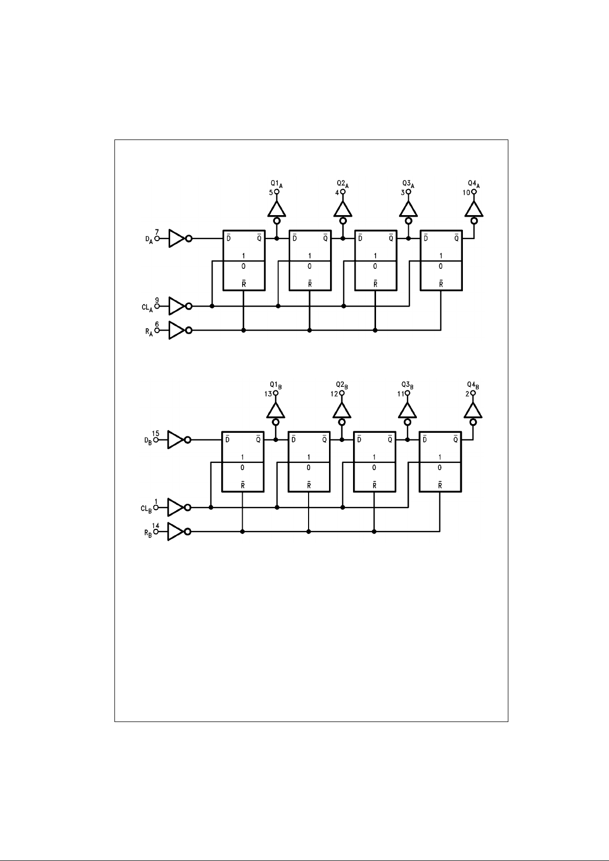
Logic Diagrams
Terminal No. 16 = V
DD
Terminal No. 8 = GND
 Loading...