


CD4027BCNMC14027BCP

October 1987
Revised January 1999
CD4027BC Dual J-K Master/Slave Flip-Flop with Set and Reset
© 1999 Fairchild Semiconductor Corporation DS005958.prf www.fairchildsemi.com
CD4027BC
Dual J-K Master/Slave Flip-Flop with Set and Reset
General Description
The CD4027BC dual J-K flip-flops are monolithic comple-
mentary MOS (CMOS) integrated circuits constructed with
N- and P-channel enhancement mode transistors. Each
flip-flop has indepe ndent J, K, set, reset, and clock inputs
and buffered Q and Q
outputs. These flip-flops ar e edge
sensitive to the clock input and change stat e on the posi-
tive-going transition of the clock pulses. Set or reset is
independent of the clock and is accomplished by a high
level on the respective input.
All inputs are protected a gainst damage due to static dis-
charge by diode clamps to V
DD
and V
SS
.
Features
■ Wide supply voltage range: 3.0V to 15V
■ High noise immunity: 0.45 V
DD
(typ.)
■ Low power TTL compatibility: Fan out of 2 driving 74L
or 1 driving 74LS
■ Low power: 50 nW (typ.)
■ Medium speed operation: 12 MHz (typ.) with 10V
supply
Ordering Code:
Devices also available in Tape and Reel. Specify by appending the suffix letter “X” to the ordering code.
Connection Diagram
Pin Assignments for DIP and SOIC
Top View
Truth Table
I = HIGH Level
O = LOW Level
X = Don't Care
= LOW-to-HIGH
= HIGH-to-LOW
Note 1: t
n−1
refers to the time interval p rior to the positive clock pulse
transition
Note 2: t
n
refers to the time intervals after the positive clock pulse
transition
Note 3: Level Change
Order Number Package Number Package Description
CD4027BCM M16A 16-Lead Small Outline Integrated Circuit (SOIC), JEDEC MS-012, 0.150” Narrow Body
CD4027BCN N16E 16-Lead Plastic Dual-In-Line Package (PDIP), JEDEC MS-001, 0.300” Wide
Inputs t
n−1
(Note 1)
Outputs t
n
(Note 2)
CL
(Note 3)
JKSRQQ Q
I XOOO I O
XOOO I I O
OXOOOO I
XIOOIO I
X X O O X (No Change)
XXXIOXI O
XXXOIXO I
XXXIIXI I
www.fairchildsemi.com 2
CD4027BC
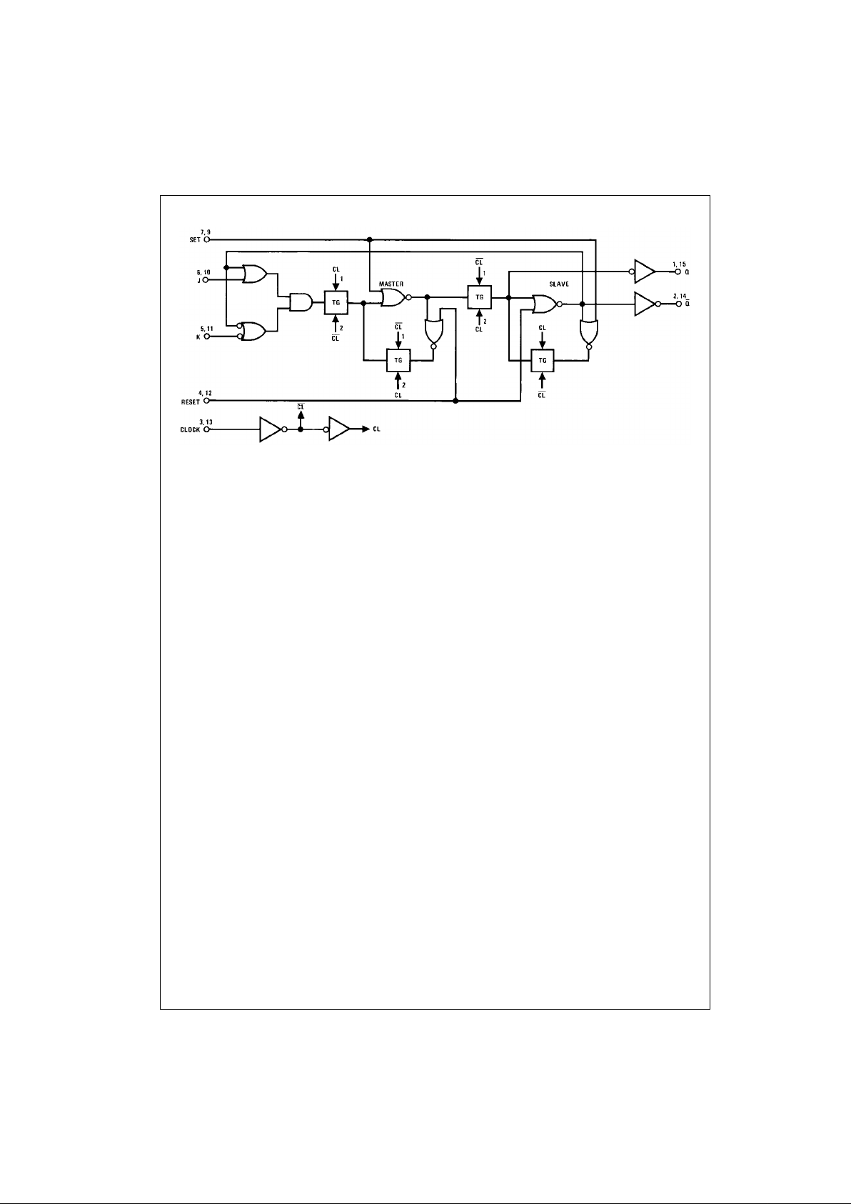
Logic Diagram
 Loading...