


October 1987
Revised May 1999
CD4047BC
Low Power Monostable/Astable Multivibrator
General Description
The CD4047B is capable of operating in either the monostable or astable mode. It requires an external capacitor (between pins 1 and 3) and an external resistor (between pins 2 and 3) to determine the output pulse width in the monostable mode, and the output frequency in the astable mode.
Astable operation is enabled by a high level on the astable input or low level on the astable input. The output frequency (at 50% duty cycle) at Q and Q outputs is determined by the timing components. A frequency twice that of Q is available at the Oscillator Output; a 50% duty cycle is not guaranteed.
Monostable operation is obtained when the device is triggered by LOW-to-HIGH transition at + trigger input or HIGH-to-LOW transition at − trigger input. The device can be retriggered by applying a simultaneous LOW-to-HIGH transition to both the + trigger and retrigger inputs.
A high level on Reset input resets the outputs Q to LOW, Q to HIGH.
Features
■Wide supply voltage range: 3.0V to 15V
■High noise immunity: 0.45 VDD (typ.)
■Low power TTL compatibility: Fan out of 2 driving 74L or 1 driving 74LS
SPECIAL FEATURES
■Low power consumption: special CMOS oscillator configuration
■Monostable (one-shot) or astable (free-running) operation
■True and complemented buffered outputs
■Only one external R and C required
MONOSTABLE MULTIVIBRATOR FEATURES
■Positiveor negative-edge trigger
■Output pulse width independent of trigger pulse duration
■Retriggerable option for pulse width expansion
■Long pulse widths possible using small RC components by means of external counter provision
■Fast recovery time essentially independent of pulse width
■Pulse-width accuracy maintained at duty cycles approaching 100%
ASTABLE MULTIVIBRATOR FEATURES
■Free-running or gatable operating modes
■50% duty cycle
■Oscillator output available
■Good astable frequency stability typical= ±2% + 0.03%/°C @ 100 kHz
frequency= ±0.5% + 0.015%/°C @ 10 kHz
deviation (circuits trimmed to frequency VDD = 10V
±10%)
Applications
•Frequency discriminators
•Timing circuits
•Time-delay applications
•Envelope detection
•Frequency multiplication
•Frequency division
Ordering Code:
Order Number |
Package Number |
Package Description |
|
|
|
CD4047BCM |
M14A |
14-Lead Small Outline Integrated Circuit (SOIC), JEDEC MS-120, 0.150” Narrow |
|
|
|
CD4047BCN |
N14A |
14-Lead Plastic Dual-In-Line Package (PDIP), JEDEC MS-001, 0.300” Wide |
|
|
|
Devices also available in Tape and Reel. Specify by appending the suffix letter “X” to the ordering code.
Multivibrator Monostable/Astable Power Low CD4047BC
© 1999 Fairchild Semiconductor Corporation |
DS005969.prf |
www.fairchildsemi.com |
CD4047BC
Connection Diagram
Pin Assignments for SOIC and DIP
Top View
Function Table
|
|
Terminal Connections |
Output Pulse |
Typical Output |
||
|
|
|
|
|
|
|
Function |
To VDD |
|
To VSS |
Input Pulse |
From |
Period or |
|
|
|
|
To |
|
Pulse Width |
|
|
|
|
|
|
|
Astable Multivibrator |
|
|
|
|
|
|
Free-Running |
4, 5, 6, 14 |
|
7, 8, 9, 12 |
|
10, 11, 13 |
tA(10, 11) = 4.40 RC |
True Gating |
4, 6, 14 |
|
7, 8, 9, 12 |
5 |
10, 11, 13 |
tA (13) = 2.20 RC |
Complement Gating |
6, 14 |
|
5, 7, 8, 9, 12 |
4 |
10, 11, 13 |
|
|
|
|
|
|
|
|
Monostable Multivibrator |
|
|
|
|
|
|
Positive-Edge Trigger |
4, 14 |
|
5, 6, 7, 9, 12 |
8 |
10, 11 |
|
Negative-Edge Trigger |
4, 8, 14 |
|
5, 7, 9, 12 |
6 |
10, 11 |
tM (10, 11) = 2.48 RC |
Retriggerable |
4, 14 |
|
5, 6, 7, 9 |
8, 12 |
10, 11 |
|
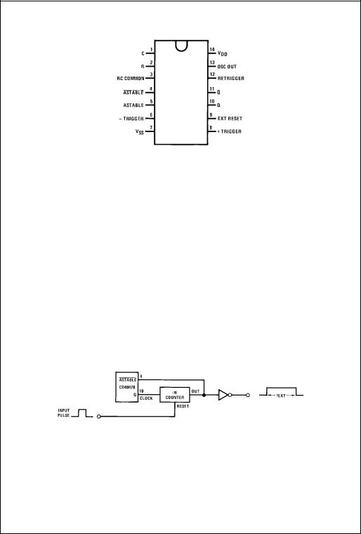
External Countdown (Note 1) |
|
|
|
|
|
|
14 |
|
5, 6, 7, 8, 9, 12 |
Figure 1 |
Figure 1 |
Figure 1 |
|
|
|
|
|
|
|
|
Note 1: External resistor between terminals 2 and 3. External capacitor between terminals 1 and 3.
Typical Implementation of External Countdown Option
tEXT = (N − 1) tA + (tM + tA/2)
FIGURE 1.
www.fairchildsemi.com |
2 |

Block Diagram
Logic Diagram
*Special input protection circuit to permit larger input-voltage swings.
CD4047BC
3 |
www.fairchildsemi.com |
 Loading...