Fairchild Semiconductor CD4043BCSJX, CD4043BCSJ, CD4043BCN, CD4043BCMX, CD4043BCM Datasheet

October 1987
Revised January 1999
CD4043BC • CD4044BC
Quad 3-STATE NOR R/S Latches •
Quad 3-STATE NAND R/S Latches
General Description
The CD4043BC are quad cross-couple 3-STATE CMOS NOR latches, and the CD4044BC are quad cross-couple 3- STATE CMOS NAND latches. Each latch has a separate Q output and individual SET and RESET inputs. There is a common 3-STATE ENABLE input for all four latches. A logic “1” on the ENABLE input connects the latch states to the Q outputs. A logic “0” on the ENABLE input disconnects the latch states from the Q outputs resulting in an open circuit condition on the Q output. The 3-STATE feature allows common bussing of the outputs.
Features
■Wide supply voltage range: 3V to 15V
■Low power: 100 nW (typ.)
■High noise immunity: 0.45 VDD (typ.)
■Separate SET and RESET inputs for each latch
■NOR and NAND configuration
■3-STATE output with common output enable
Applications
•Multiple bus storage
•Strobed register
•Four bits of independent storage with output enable
•General digital logic
Ordering Code:
Order Number |
Package Number |
Package Description |
|
|
|
CD4043BCM |
M16A |
16-Lead Small Outline Integrated Circuit (SOIC), JEDEC MS-012, 0.150” Narrow Body |
|
|
|
CD4043BCN |
N16E |
16-Lead Plastic Dual-In-Line Package (PDIP), JEDEC MS-001, 0.300” Wide |
|
|
|
CD4044BCM |
M16A |
16-Lead Small Outline Integrated Circuit (SOIC), JEDEC MS-012, 0.150” Narrow Body |
|
|
|
CD4044BCSJ |
M16D |
16-Lead Small Outline Package (SOP), EIAJ TYPE II, 5.3mm Wide |
|
|
|
CD4044BCN |
N16E |
16-Lead Plastic Dual-In-Line Package (PDIP), JEDEC MS-001, 0.300” Wide |
|
|
|
Devices also available in Tape and Reel. Specify by appending the suffix letter “X” to the ordering code.
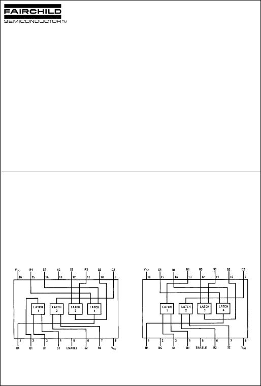
Connection Diagrams
Pin Assignments for DIP, SOIC and SOP |
Pin Assignments for DIP and SOIC |
CD4043BC |
CD4044BC |
Top View |
Top View |
Latches R/S NAND STATE-3 Quad • Latches R/S NOR STATE-3 Quad CD4044BC • CD4043BC
© 1999 Fairchild Semiconductor Corporation |
DS005967.prf |
www.fairchildsemi.com |

CD4043BC • CD4044BC
Block Diagrams
CD4043BC
Truth Tables
CD4043BC
S |
R |
E |
Q |
|
|
|
|
X |
X |
0 |
OC |
0 |
0 |
1 |
NC |
1 |
0 |
1 |
1 |
0 |
1 |
1 |
0 |
1 |
1 |
1 |
|
|
|
|
|
OC = 3-STATE
NC = No change
X = Don’t care
=Dominated by S = 1 input
=Dominated by R = 0 input
CD4044BC
CD4044BC
S |
R |
E |
Q |
|
|
|
|
X |
X |
0 |
OC |
1 |
1 |
1 |
NC |
0 |
1 |
1 |
1 |
1 |
0 |
1 |
0 |
0 |
0 |
1 |
|
|
|
|
|
www.fairchildsemi.com |
2 |
 Loading...