


CD4071BCN
October 1987
Revised January 1999
CD4071BC • CD4081BC Quad 2-Input OR Buffered B Series Gate • Quad 2-Input AND Buffered B Series Gate
© 1999 Fairchild Semiconductor Corporation DS005977.prf www.fairchildsemi.com
CD4071BC • CD4081BC
Quad 2-Input OR Buffered B Series Gate •
Quad 2-Input AND Buffered B Series Gate
General Description
The CD4071BC and CD4081BC quad gates are monolithic
complementary MOS (CMOS) integrated circuits constructed with N- and P-ch annel enhancement mode transistors. They have equal source and sink current
capabilities and conform to standard B series output drive.
The devices also have buffered outputs which improve
transfer characteristics by providing very high gain.
All inputs protected a gainst stati c discharg e with dio des to
V
DD
and VSS.
Features
■ Low power TTL compatibility:
Fan out of 2 driving 74L or 1 driving 74LS
■ 5V–10V–15V parametric ratings
■ Symmetrical output characteristics
■ Maximum input leakage 1 µA at 15V over full
temperat ure range
Ordering Code:
Devices are also available in Tape and Reel. Specify by appending the suffix letter “X ” t o t he ordering code.
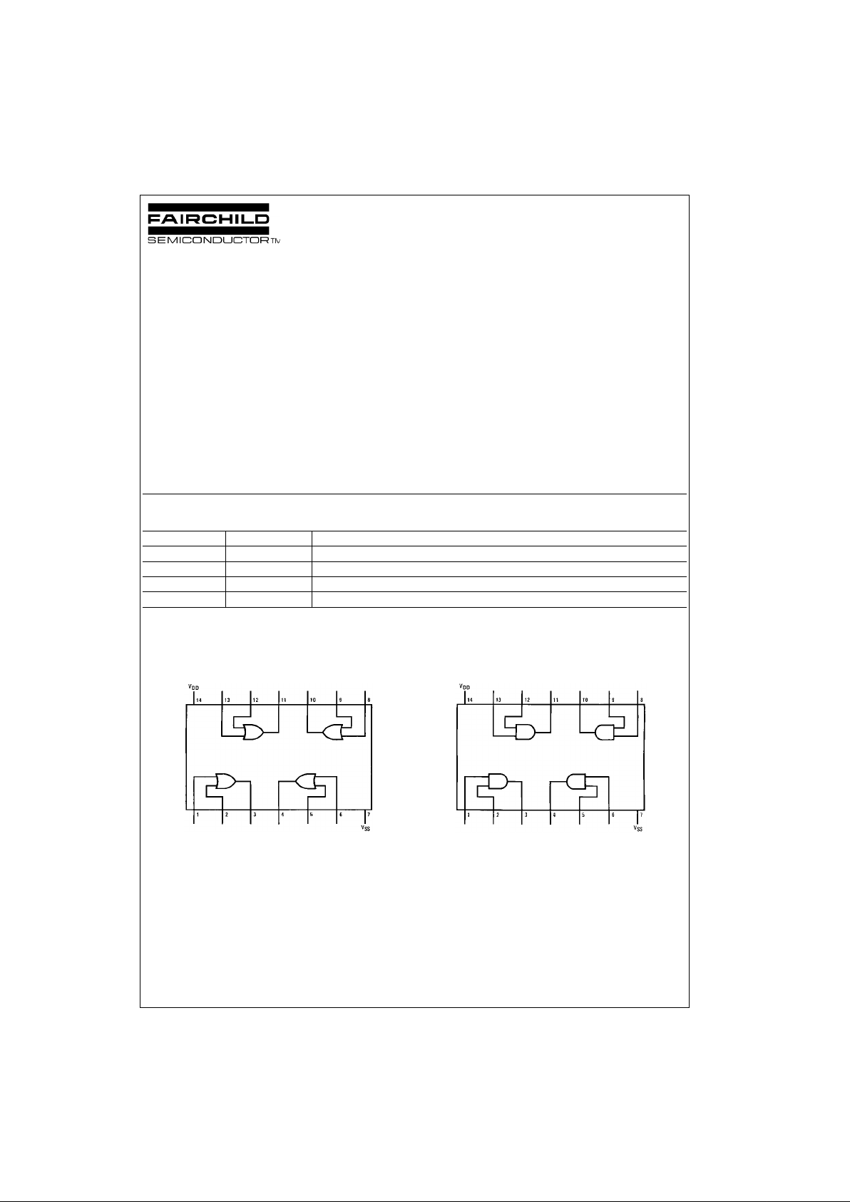
Connection Diagrams
Pin Assignments for DIP and SOIC
CD4071B
Top View
CD4081B
Top Vi ew
Order Number Package Number Package Description
CD4071BCM M14A 14-Lead Small Outline Integrated Circuit (SOIC), JEDEC MS-120, 0.150” Narrow
CD4071BCN N14A 14-Lead Plastic Dual-In-Line Package (PDIP), JEDEC MS-001, 0.300” Wide
CD4081BCM M14A 14-Lead Small Outline Integrated Circuit (SOIC), JEDEC MS-120, 0.150” Narrow
CD4081BCN N14A 14-Lead Plastic Dual-In-Line Package (PDIP), JEDEC MS-001, 0.300” Wide
www.fairchildsemi.com 2
CD4071BC • CD4081BC
Schematic Diagrams
CD4071B
1
/4 of device shown
J = A + B
Logical “1” = HIGH
Logical “0” = LOW
*All inputs protected by sta ndard CMOS protect ion circuit.
CD4081B
1
/4 of device shown
J = A • B
Logical “1” = HIGH
Logical “0” = LOW
All inputs protected by st andard CMOS protect ion circuit.
3 www.fairchildsemi.com
CD4071BC • CD4081BC
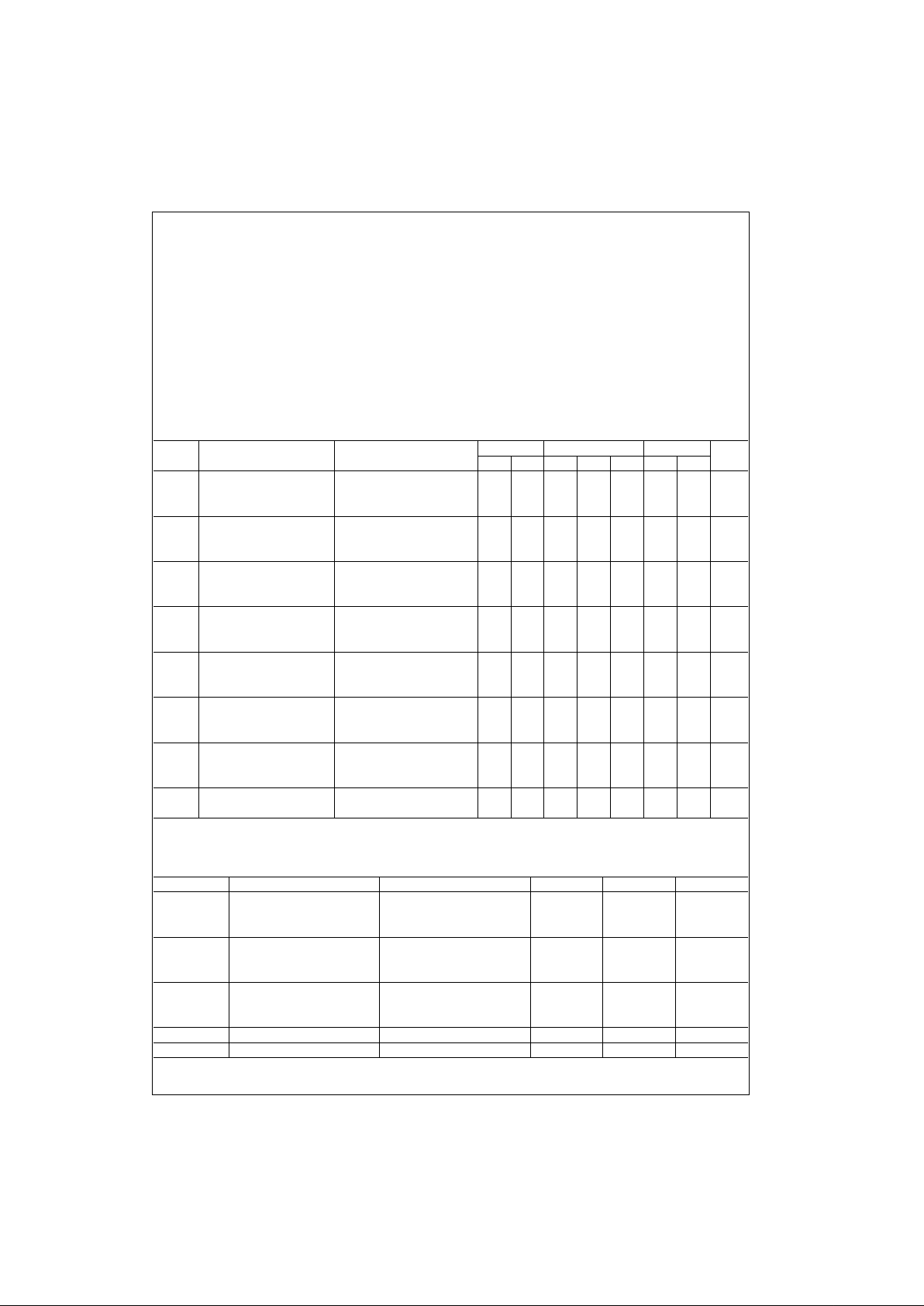
Absolute Maximum Ratings(Note 1)
(Note 2)
Recommended Operating
Conditions
Note 1: “Absolute Maximum Rat ings” are tho se values beyond which the
safety of the device cannot be guaranteed. E x c ept for “ Operating Temperature Range” they are not mea nt to imply that the devices sh ould be operated at these limits. The table of “Electrical Characteristics” provides
conditions for actual device o peration.
Note 2: All voltages measured with res pect t o V
SS
unless otherwise s peci-
fied.
DC Electrical Characteristics (Note 2)
CD4071BC/CD4081BC
Note 3: IOH and IOL are tested one output at a ti m e.
AC Electrical Characteristics (Note 4)
CD4071BC TA = 25°C, Input tr; tf = 20 ns, CL = 50 pF, RL = 200 kΩ, Typical temperature coefficient is 0.3%/°C
Note 4: AC Parameters are guaranteed by DC correlated testing.
Voltage at Any Pin −0.5V to VDD +0.5V
Power Dissipation (P
D
)
Dual-In-Line 700 mW
Small Outline 500 mW
V
DD
Range −0.5 VDC to +18 V
DC
Storage Temperature (TS) −65°C to +150°C
Lead Temperature (T
L
)
(Soldering, 10 seconds ) 260°C
Operating Range (V
DD
)3 V
DC
to 15 V
DC
Operating Temperature Range (TA)
CD4071BC, CD4081BC −40°C to +85°C
Symbol Parameter Conditions
−40°C +25°C +85°C
Units
Min Max Min Typ Max Min Max
I
DD
Quiescent Device VDD = 5V 1 0.004 1 7.5 µA
Current VDD = 10V 2 0.005 2 15 µA
VDD = 15V 4 0.006 4 30 µA
V
OL
LOW Level VDD = 5V 0.05 0 0.05 0.05 V
Output Voltage VDD = 10V |IO| < 1 µA 0.05 0 0.05 0.05 V
VDD = 15V 0.05 0 0.05 0.05 V
V
OH
HIGH Level VDD = 5V 4.95 4.95 5 4.95 V
Output Voltage VDD = 10V |IO| < 1 µA 9.95 9.95 10 9.95 V
VDD = 15V 14.95 14.95 15 14.95 V
V
IL
LOW Level VDD = 5V, VO = 0.5V 1.5 2 1.5 1.5 V
Input Voltage VDD = 10V, VO = 1.0V 3.0 4 3.0 3.0 V
VDD = 15V, VO = 1.5V 4.0 6 4.0 4.0 V
V
IH
HIGH Level VDD = 5V, VO = 4.5V 3.5 3.5 3 3.5 V
Input Voltage VDD = 10V, VO = 9.0V 7.0 7.0 6 7.0 V
VDD = 15V, VO = 13.5V 11.0 11.0 9 11.0 V
I
OL
LOW Level Output VDD = 5V, VO = 0.4V 0.52 0.44 0.88 0.36 mA
Current VDD = 10V, VO = 0.5V 1.3 1.1 2.25 0.9 mA
(Note 3) VDD = 15V, VO = 1.5V 3.6 3.0 8.8 2.4 mA
I
OH
HIGH Level Output VDD = 5V, VO = 4.6V −0.52 −0.44 −0.88 −0.36 mA
Current VDD = 10V, VO = 9.5V −1.3 −1.1 −2.25 −0.9 mA
(Note 3) VDD = 15V, VO = 13.5V −3.6 −3.0 −8.8 −2.4 mA
I
IN
Input Current VDD = 15V, VIN = 0V −0.30 −10−5−0.30 −1.0 µA
VDD = 15V, VIN = 15V 0.30 10−50.30 1.0 µA
Symbol Parameter Conditions Typ Max Units
t
PHL
Propagation Delay Time, VDD = 5V 100 250 ns
HIGH-to-LOW Lev el VDD = 10V 40 100 ns
VDD = 15V 3070ns
t
PLH
Propagation Delay Time, VDD = 5V 90 250 ns
LOW-to-HIGH Le vel VDD = 10V 40 100 ns
VDD = 15V 3070ns
t
THL
, t
TLH
Transition Time VDD = 5V 90 200 ns
VDD = 10V 50 100 ns
VDD = 15V 4080ns
C
IN
Average Input Capacitance Any Input 5 7.5 pF
C
PD
Power Dissipation Capacity Any Gate 18 pF
 Loading...