Fairchild Semiconductor CD40174BCN, CD40174BCMX, CD40174BCM Datasheet

October 1987
Revised July 1999
CD40174BC • CD40175BC
Hex D-Type Flip-Flop • Quad D-Type Flip-Flop
General Description
The CD40174BC consists of six positive-edge triggered D- type flip-flops; the true outputs from each flip-flop are externally available. The CD40175BC consists of four positiveedge triggered D-type flip-flops; both the true and complement outputs from each flip-flop are externally available.
All flip-flops are controlled by a common clock and a common clear. Information at the D inputs meeting the set-up time requirements is transferred to the Q outputs on the positive-going edge of the clock pulse. The clearing operation, enabled by a negative pulse at Clear input, clears all Q outputs to logical “0” and Q s (CD40175BC only) to logical “1”.
All inputs are protected from static discharge by diode clamps to VDD and VSS.
Features
■Wide supply voltage range: 3V to 15V
■High noise immunity: 0.45 VDD (typ.)
■Low power TTL compatibility:
fan out of 2 driving 74L or 1 driving 74 LS
■Equivalent to MC14174B, MC14175B
■Equivalent to MM74C174, MM74C175
Ordering Code:
Order Number |
Package Number |
Package Description |
|
|
|
CD40174BCM |
M16A |
16-Lead Small Outline Integrated Circuit (SOIC), JEDEC MS-012, 0.150” Narrow Body |
|
|
|
CD40174BCN |
N16E |
16-Lead Plastic Dual-In-Line Package (PDIP), JEDEC MS-001, 0.300” Wide |
|
|
|
CD40175BCM |
M16A |
16-Lead Small Outline Integrated Circuit (SOIC), JEDEC MS-012, 0.150” Narrow Body |
|
|
|
CD40175BCN |
N16E |
16-Lead Plastic Dual-In-Line Package (PDIP), JEDEC MS-001, 0.300” Wide |
|
|
|
Devices also available in Tape and Reel. Specify by appending the suffix letter “X” to the ordering code.
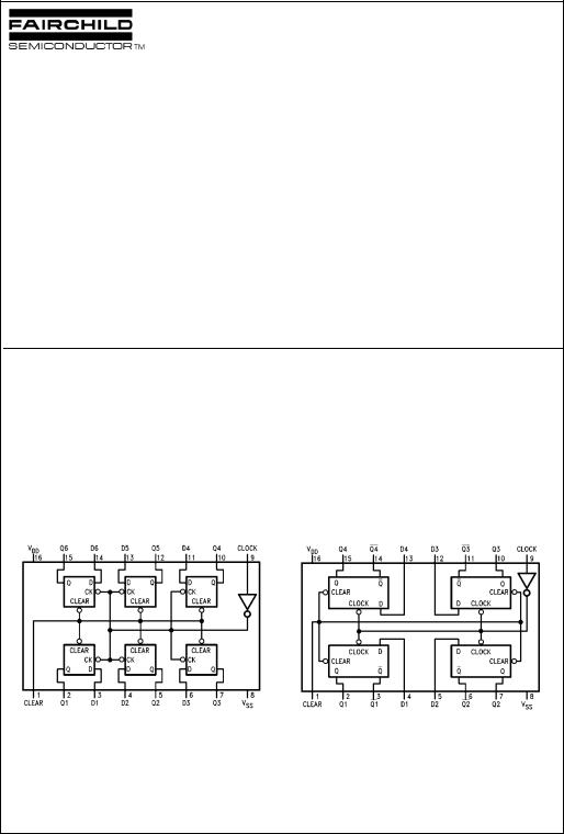
Connection Diagrams
Pin Assignments for DIP and SOIC
CD40174B |
CD40175B |
Top View |
Top View |
Flop-Flip Type-D Quad • Flop-Flip Type-D Hex CD40175BC • CD40174BC
© 1999 Fairchild Semiconductor Corporation |
DS005987 |
www.fairchildsemi.com |

CD40174BC • CD40175BC
Truth Table
|
Inputs |
|
|
Outputs |
||
|
|
|
|
|
|
|
Clear |
Clock |
D |
Q |
|
Q |
|
|
|
|
|
(Note 1) |
||
|
|
|
|
|
|
|
L |
X |
X |
L |
|
H |
|
H |
− |
H |
H |
|
L |
|
H |
− |
L |
L |
|
H |
|
H |
H |
X |
NC |
NC |
||
H |
L |
X |
NC |
NC |
||
H = HIGH Level
L = LOW Level
X = Irrelevant
− = Transition from LOW-to-HIGH level NC = No change
Note 1: Q for CD40175B only
www.fairchildsemi.com |
2 |

|
Storage Temperature Range (T ) |
|
|
−65°C to +150°C |
|
Input Voltage (VIN) |
|
|
|
|
0V to VDD VDC |
CD40174BC |
||||||||||
|
Absolute Maximum Ratings(Note 2) |
|
Recommended Operating |
|
|
|||||||||||||||||
|
(Note 3) |
|
|
|
|
|
|
|
|
|
Conditions (Note 3) |
|
|
|
|
|
||||||
|
DC Supply Voltage (VDD) |
|
|
−0.5V to +18V |
|
|
|
|
|
|
|
|
|
|
|
|
||||||
|
Input Voltage (V ) |
−0.5V to V |
DD |
+0.5V |
DC |
|
DC Supply Voltage (VDD) |
|
|
|
3V to 15 VDC |
|
||||||||||
|
|
|
IN |
|
|
|
|
|
|
|
|
|
|
|
|
|
|
|
|
|||
|
|
|
S |
|
|
|
|
|
|
|
|
|
|
|
|
|
|
|
−40°C to +85°C |
• |
||
|
Power Dissipation (P ) |
|
|
|
|
|
|
|
|
Operating Temperature Range (TA) |
||||||||||||
|
|
|
|
|
|
|
|
|
CD40175BC |
|||||||||||||
|
|
|
D |
|
|
|
|
|
|
|
|
|
|
|
|
|
|
|
|
|
|
|
|
|
|
|
|
|
|
|
|
|
|
|
|
|
|
|
|
|
|
|
|
|
|
|
Dual-In-Line |
|
|
|
|
|
700 mW |
Note 2: “Absolute Maximum Ratings” are those values beyond which the |
|
|||||||||||||
|
Small Outline |
|
|
|
|
|
500 mW |
safety of the device cannot be guaranteed. They are not meant to imply |
|
|||||||||||||
|
|
|
|
|
|
that the devices should be operated at these limits. The tables of “Recom- |
|
|||||||||||||||
|
Lead Temperature (TL) |
|
|
|
|
|
|
|
mended Operating Conditions” and “Electrical Characteristics” provide con- |
|
||||||||||||
|
|
|
|
|
|
|
|
ditions for actual device operation. |
|
|
|
|
|
|
|
|||||||
|
(Soldering, 10 seconds) |
|
|
|
|
|
260°C |
|
|
|
|
|
|
|
||||||||
|
|
|
|
|
|
Note 3: VSS = 0V unless otherwise specified. |
|
|
|
|
|
|||||||||||
|
|
|
|
|
|
|
|
|
|
|
|
|
|
|
|
|||||||
|
DC Electrical Characteristics (Note 3) |
|
|
|
|
|
|
|
|
|
|
|
|
|||||||||
|
CD40174BC/CD40175BC |
|
|
|
|
|
|
|
|
|
|
|
|
|
|
|
|
|
|
|
||
|
Symbol |
|
Parameter |
|
|
Conditions |
|
|
−40°C |
|
+25°C |
|
+85°C |
Units |
|
|||||||
|
|
|
|
|
|
|
|
|
|
|
|
|
|
|
||||||||
|
|
|
|
|
|
|
|
|
|
|
|
|
Min |
Max |
Min |
Typ |
|
Max |
Min |
Max |
|
|
|
|
|
|
|
|
|
|
|
|
|
|
|
|
|
|
|||||||
IDD |
|
Quiescent Device |
VDD = 5V, VIN = VDD or VSS |
|
|
|
4 |
|
|
|
4 |
|
30 |
μA |
|
|||||||
|
|
|
Current |
VDD = 10V, VIN = VDD or VSS |
|
|
|
8 |
|
|
|
8 |
|
60 |
μA |
|
||||||
|
|
|
|
VDD = 15V, VIN = VDD or VSS |
|
|
|
16 |
|
|
|
16 |
|
120 |
μA |
|
||||||
VOL |
|
LOW Level |
VDD = 5V |
|
|
|
|
|
|
|
0.05 |
|
|
|
0.05 |
|
0.05 |
V |
|
|||
|
|
|
Output Voltage |
VDD = 10V |
|
|
|
|
|
|
|
0.05 |
|
|
|
0.05 |
|
0.05 |
V |
|
||
|
|
|
|
VDD = 15V |
|
|
|
|
|
|
|
0.05 |
|
|
|
0.05 |
|
0.05 |
V |
|
||
VOH |
|
HIGH Level |
VDD = 5V |
|
|
|
|
|
|
4.95 |
|
4.95 |
5 |
|
|
4.95 |
|
V |
|
|||
|
|
|
Output Voltage |
VDD = 10V |
|
|
|
|
|
|
9.95 |
|
9.95 |
10 |
|
|
9.95 |
|
V |
|
||
|
|
|
|
VDD = 15V |
|
|
|
|
|
|
14.95 |
|
14.95 |
15 |
|
|
14.95 |
|
V |
|
||
VIL |
|
LOW Level |
VDD = 5V, VO = 0.5V or 4.5V |
|
|
|
1.5 |
|
|
|
1.5 |
|
1.5 |
V |
|
|||||||
|
|
|
Input Voltage |
VDD = 10V, VO = 1V or 9V |
|
|
|
3.0 |
|
|
|
3.0 |
|
3.0 |
V |
|
||||||
|
|
|
|
VDD = 15V, VO = 1.5V or 13.5V |
|
|
4.0 |
|
|
|
4.0 |
|
4.0 |
V |
|
|||||||
VIH |
|
HIGH Level |
VDD = 5V, VO = 0.5V or 4.5V |
|
|
3.5 |
|
3.5 |
|
|
|
3.5 |
|
V |
|
|||||||
|
|
|
Input Voltage |
VDD = 10V, VO = 1V or 9V |
|
|
7.0 |
|
7.0 |
|
|
|
7.0 |
|
V |
|
||||||
|
|
|
|
VDD = 15V, VO = 1.5V or 13.5V |
|
11.0 |
|
11.0 |
|
|
|
11.0 |
|
V |
|
|||||||
IOL |
|
LOW Level Output |
VDD = 5V, VO = 0.4V |
|
|
|
0.52 |
|
0.44 |
0.88 |
|
|
0.36 |
|
mA |
|
||||||
|
|
|
Current (Note 4) |
VDD = 10V, VO = 0.5V |
|
|
|
1.3 |
|
1.1 |
2.25 |
|
|
0.9 |
|
mA |
|
|||||
|
|
|
|
VDD = 15V, VO = 1.5V |
|
|
|
3.6 |
|
3.0 |
8.8 |
|
|
2.4 |
|
mA |
|
|||||
IOH |
|
HIGH Level Output |
VDD = 5V, VO = 4.6V |
|
|
|
−0.52 |
|
−0.44 |
−0.88 |
|
|
−0.36 |
|
mA |
|
||||||
|
|
|
Current (Note 4) |
VDD = 10V, VO = 9.5V |
|
|
|
−1.3 |
|
−1.1 |
−2.25 |
|
|
−0.9 |
|
mA |
|
|||||
|
|
|
|
VDD = 15V, VO = 13.5V |
|
|
|
−3.6 |
|
−3.0 |
−8.8 |
|
|
−2.4 |
|
mA |
|
|||||
I |
IN |
|
Input Current |
V |
DD |
= 15V, V |
IN |
= 0V |
|
|
|
|
−0.30 |
|
−10−5 |
|
−0.30 |
|
−1.0 |
μA |
|
|
|
|
|
|
|
|
|
|
|
|
|
|
|
|
|
|
|
|
|
|
|||
|
|
|
|
V |
DD |
= 15V, V |
IN |
= 15V |
|
|
|
|
0.30 |
|
10−5 |
|
0.30 |
|
1.0 |
μA |
|
|
|
|
|
|
|
|
|
|
|
|
|
|
|
|
|
|
|
|
|
|
|
||
|
Note 4: IOH and IOL are tested one output at a time. |
|
|
|
|
|
|
|
|
|
|
|
|
|
|
|
|
|
||||
|
|
|
|
|
|
|
|
|
|
|
|
|
|
|
|
|
|
|
|
|
|
|
3 |
www.fairchildsemi.com |
 Loading...