


CD4538BCWMX
Fairchild Semiconductor CD4538BCWMX, CD4538BCWM, CD4538BCN, CD4538BCMX, CD4538BCM Datasheet
...
October 1987
Revised January 1999
CD4538BC Dual Precision Monostable
© 1999 Fairchild Semiconductor Corporation DS006000.prf www.fairchildsemi.com
CD4538BC
Dual Precision Monostable
General Description
The CD4538BC is a dual, precision monostable multivibrator with independent t ri gger and re set con trols. The device
is retriggerable and resettable, and the contro l inputs are
internally latched. Two trigger inputs are provided to allow
either rising or falling edge triggering. The reset inputs are
active LOW and prevent triggering while active. Precise
control of output pulse-w idth has been achieved using linear CMOS techniques. The pu lse duration and accuracy
are determined by exter nal components R
X
and CX. The
device does not allow the timing capacitor to discharge
through the timing pi n on power-down condition. For this
reason, no external protect ion resistor is r equire d in se ries
with the timing pin. Input protection from static discharge is
provided on all pins.
Features
■ Wide supply voltage range: 3.0V to 15V
■ High noise immunity: 0.45 V
CC
(typ.)
■ Low power TTL compatibility: Fan out of 2 driving 74L
or 1 driving 74LS
■ New formula: PW
OUT
= RC (PW in seconds, R in Ohms,
C in Farads)
■ ±1.0% pulse-width variation from part to part (typ.)
■ Wide pulse-width range: 1 µs to ∞
■ Separate latched reset inputs
■ Symmetrical output sink and source capability
■ Low standby current: 5 nA (typ.) @ 5 V
DC
■ Pin compatible to CD4528BC
Ordering Code:
Devices also available in Tape and Reel. Specify by appending the suffix letter “X” to t he ordering code.
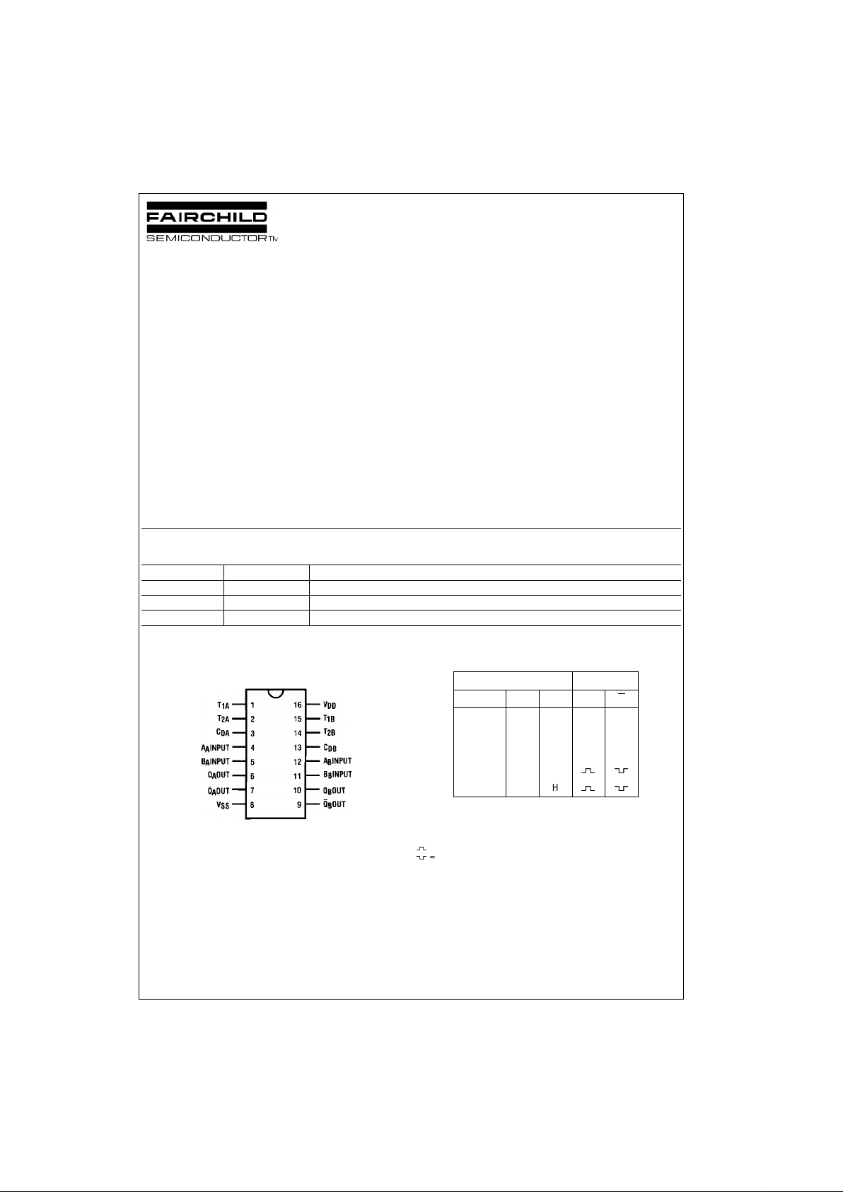
Connection Diagram
Pin Assignments for DIP and SOIC
Top View
Truth Table
H = HIGH Level
L = LOW Level
↑ = Transition from LOW-to-HIGH
↓ = Transition from HIGH-to-LOW
= One HIGH Level Pulse
= One LOW Level Pulse
X = Irrelevant
Order Number Package Number Package Description
CD4538BCM M16A 16-Lead Small Outline Integrated Circuit (SOIC), JEDEC MS-012, 0.150” Narrow Body
CD4538BCWM M16B 16-Lead Small Outline Integrated Circuit (SOIC), JEDEC MS-013, 0.300” Wide Body
CD4538BCN N16E 16-Lead Plastic Dual-In-Line Package (PDIP), JEDEC MS-001, 0.300” Wide
Inputs Outputs
Clear A B Q Q
LXXLH
XHXLH
XXLLH
HL↓
H ↑ H
www.fairchildsemi.com 2
CD4538BC
Block Diagram
RX and CX are External Com ponents
V
DD
= Pin 16
V
SS
= Pin 8
Logic Diagram
FIGURE 1.
3 www.fairchildsemi.com
CD4538BC
Theory of Operation
FIGURE 2.
Trigger Operation
The block diagram of the CD4538B C is shown in Figure 1,
with circuit operation following.
As shown in Figure 1 and Fi gure 2, before an in put tr igger
occurs, the monostable is in the quiescent stat e with the Q
output low, and the timing capacitor C
X
completely charged
to V
DD
. When the trigger input A goes from VSS to V
DD
(while inputs B and CD are held to VDD) a valid trigger is
recognized, which turns on compara tor C1 and N-Chan nel
transistor N1
(1)
. At the same time the outp ut latch is set.
With transistor N1 on, the ca pacitor C
X
rapidly discharges
toward V
SS
until V
REF1
is reached. At th is point th e output
of comparator C1 changes state and transistor N1 turns off.
Comparator C1 then tu rn s off w hile at the sa me ti me com parator C2 turns on. With transistor N1 off, the capacitor C
X
begins to charge thr ough the timing resistor, RX, toward
V
DD
. When the voltage across CX equals V
REF2
, compara-
tor C2 changes state causing the output latch to reset (Q
goes low) while at the same time disabling comparator C2.
This ends the timing cycle with the mono stable in the quiescent state, waiting for the next trigger.
A valid trigger is also recognized when trigger input B goes
from V
DD
to VSS (while input A is at VSS and input CD is at
V
DD
)
(2)
.
It should be noted that in the quiescent state C
X
is fully
charged to V
DD
, causing the current throu gh res istor RX to
be zero. Both comparators are “off” wi th the total device
current due only to r everse junction leakages. An a dded
feature of the CD4538BC is that th e output latch is set via
the input trigger withou t regard to the capacitor voltage.
Thus, propagation delay from trigger to Q is independent of
the value of C
X
, RX, or the duty cycle of the inpu t wave-
for m.
Retrigger Operation
The CD4538BC is retriggered if a valid trigger occurs
(3)
fol-
lowed by another valid t rigger
(4)
before the Q output has
returned to the quiescent (zero) state. Any retrigger, after
the timing node voltage at pin 2 or 14 has begun to r ise
from V
REF1
, but has not yet reached V
REF2
, will cause an
increase in output pulse width T. When a valid retrigger is
initiated
(4)
, the voltage at T2 will again drop to V
REF1
before
progressing along the RC charg ing cur ve toward V
DD
. The
Q output will remain high until time T, after the last valid
retrigger.
Reset Operation
The CD4538BC may be reset dur ing t he generatio n of the
output pulse. In the reset mode of operation, an input pulse
on C
D
sets the reset latch an d causes the c apacitor to be
fast charged to V
DD
by turning on transistor Q1
(5)
. When
the voltage on the capacitor r each es V
REF2
, the reset latch
will clear and then be ready to accept another pulse. If the
C
D
input is held low, any trigger inputs that occur will be
inhibited and the Q and Q
outputs of the output la tch will
not change. Since the Q output is reset when an input low
level is detected on the C
D
input, the output pulse T can be
made significantly shor ter than the minimum pulse width
specification.
www.fairchildsemi.com 4
CD4538BC
FIGURE 3. Retriggerable Monostables Circuitry
FIGURE 4. Non-Retriggerable Monostables Circuitry
FIGURE 5. Connection of Unused Sections
 Loading...