Texas Instruments TRF7961RHBT, TRF7961, TRF7960, TRF7960RHBT Datasheet

TRF7960/61
www.ti.com |
SLOS504B – AUGUST 2006 – REVISED APRIL 2007 |
|
Multi-Standard Fully Integrated 13.56-MHz Radio Frequency Identification (RFID) Analog
Front End and Data Framing Reader System
FEATURES
∙Completely Integrated Protocol Handling (OSI Model Layer 3 and Below)
∙Separate Internal High-PSRR Power Supplies for Analog, Digital, and PA Sections Provides Noise Isolation for Superior Read Range and Reliability
∙Dual Receiver Input With AM and PM Demodulation to Minimize Communication Holes (Patent Pending).
∙Receiver AM and PM RSSI
∙Reader-to-Reader Anti-Collision
∙High Integration Reduces Total BOM and Board Area
–Single External 13.56-MHz Cystal Oscillator
–MCU-Selectable Clock-Fequency Output of RF, RF/2, or RF/4
–Adjustable 20-mA, High-PSRR LDO for Powering External MCU
∙Easy to Use With High Flexibility
–Auto-Configured Default Modes for Each Spported ISO Protocol
–11 User-Programmable Registers
–Selectable Receiver Gain and AGC
–Programmable Output Power (100 mW or 200 mW)
–Adjustable ASK Modulation Range (8% to 30%)
–Built-In Receiver Band-Pass Filter With User-Selectable Corner Frequencies
∙Wide Operating Voltage Range of 2.7 V to 5.5 V
∙Ultralow-Power Modes
–Power Down < 1 μA
–Standby 120 μA
–Active (Rx only) 10 mA
∙Parallel 8-Bit or Serial 4-Pin SPI Interface With MCU Using 12-Byte FIFO
∙Ultrasmall 32-Pin QFN Package (5 mm ×
5 mm)
∙Available tools
–Reference Design/EVM With Development Software
–Source Code Available for MSP430
APPLICATIONS
∙Secure Access Control
∙Product Authentication
–Printer Ink Cartridges
–Blood Gucose Monitors
∙Contactless Payment Systems
DESCRIPTION
The TRF7960/61 is an integrated analog front end and data framing system for a 13.56-MHz RFID reader system. Built-in programming options make it suitable for a wide range of applications both in proximity and vicinity RFID systems.
The reader is configured by selecting the desired protocol in the control registers. Direct access to all control registers allows fine tuning of various reader parameters as needed.
Table 1. PRODUCT SELECTION TABLE
|
|
|
PROTOCOLS |
|
|
|
DEVICE |
|
ISO14443A/B |
|
ISO15693 |
Tag-it™ |
|
|
106 kbps |
212 kbps |
424 kbps |
848 kbps |
ISO18000-3 |
|
|
|
|||||
TRF7960 |
X |
X |
X |
X |
X |
X |
TRF7961 |
|
|
|
|
X |
X |
Please be aware that an important notice concerning availability, standard warranty, and use in critical applications of Texas Instruments semiconductor products and disclaimers thereto appears at the end of this data sheet.
Tag-it is a trademark of Texas Instruments Incorporated.
PRODUCTION DATA information is current as of publication date. |
Copyright © 2006–2007, Texas Instruments Incorporated |
Products conform to specifications per the terms of the Texas |
|
Instruments standard warranty. Production processing does not |
|
necessarily include testing of all parameters. |
|

TRF7960/61
www.ti.com
SLOS504B – AUGUST 2006 – REVISED APRIL 2007
These devices have limited built-in ESD protection. The leads should be shorted together or the device placed in conductive foam during storage or handling to prevent electrostatic damage to the MOS gates.
DESCRIPTION (CONTINUED)
|
|
|
|
|
|
|
|
|
|
|
|
SYS_CLK |
|
|
|
|
|
|
|
|
|
|
|
|
|
|
|
|
|
||
|
|
|
|
|
|
|
|
|
|
|
|
|
|
||
|
|
|
|
|
|
|
VDD_X |
|
|
VDD |
|||||
|
Z-Matching |
|
|
|
Tx_Out |
|
|
DATA_CLK |
|
|
|||||
|
Circuit |
|
|
|
|
|
|
|
|
|
|||||
|
|
|
|
TRF7960 |
|
|
IRQ |
|
|
MSP430 |
|||||
|
|
|
|
|
|
|
|
|
|
|
|||||
|
|
|
|
|
|
|
Rx1_AM |
|
|
3 (SPI) |
|
|
|||
|
|
|
|
|
|
|
|
|
|
|
|
|
|||
|
|
|
|
|
|
|
Rx2_PM |
|
|
|
|
|
|
||
|
|
|
|
|
|
|
|
|
|
|
|
|
|||
|
|
|
|
|
|
|
|
|
VDD_I/O |
|
|
8 (Parallel) |
|
|
|
|
|
|
|
|
|
|
|
|
|
|
|
|
|
||
|
|
|
|
|
|
|
|
|
|
|
|
|
|
|
|
|
|
|
|
|
|
|
|
|
|
|
|
|
|
|
|
Xtal 13.56 MHz
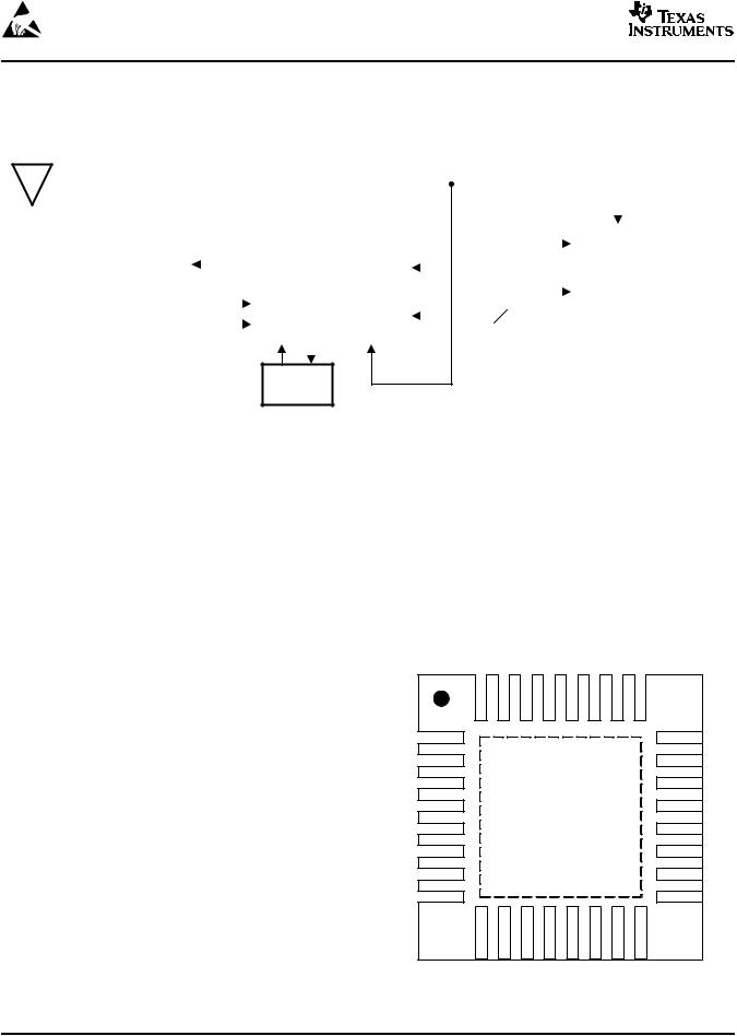
Figure 1. Typical Application
A parallel or serial interface can be used for communication between the MCU and reader. When hardware encoders and decoders are used (accelerators for different standards), transmission and receive functions use a 12-byte FIFO register. For direct transmit or receive functions, the encoders/decoders can be bypassed in order for the MCU to process the data in real time. The transmitter has selectable output-power levels of 100 mW (20 dBm) or 200 mW (23 dBm) into a 50-Ω load (at 5 -V supply) and is capable of ASK or OOK modulation. Integrated voltage regulators ensure power-supply noise rejection for the complete reader system.
Data transmission comprises low-level encoding for ISO15693, modified Miller for ISO14443-A, high-bit-rate systems, Tag-it, and HF-EPC system coding. Included with the data encoding is automatic generation of SOF, EOF, CRC, and/or parity bits.
The receiver system enables AM and PM demodulation using a dual-input architecture. The receiver also includes an automatic gain control option and selectable gain. Also included is a selectable bandwidth to cover a broad range of input subcarrier signal options. The received signal strength for AM and PM modulation is accessible via the RSSI register. The receiver output is selectable between a digitized subcarrier signal and any of eleven integrated subcarrier decoders (two for ISO15693 low bit rate, two for ISO15693 high bit rate, two for ISO14443, three for ISO14443 high bit rates, one for Tag-it, and one for HF-EPC system). Selected decoders also deliver bit stream and a data clock as outputs.
The receiver system also includes a framing system. This system performs the CRC and/or parity check, removes the EOF and SOF settings, and organizes the data in bytes. Framed data is then accessible to the MCU via a 12-byte FIFO register and MCU interface. The framing supports ISO14443 and ISO15693 protocols.
The TRF7960/61 supports data communication levels between 1.8 V–5.5 V for the MCU I/O interface while also providing a data synchronization clock. An auxiliary 20-mA regulator (pin 32) is available for additional system circuits.
|
32 |
31 |
30 |
29 |
28 |
27 |
26 |
25 |
|
|
VDD X |
OSC IN |
OSC OUT |
VSS D |
EN |
SYS CLK |
DATA CLK |
EN2 |
|
1 |
VDD_A |
|
|
|
|
|
|
I/O_7 |
24 |
2 |
VIN |
|
|
|
|
|
|
I/O_6 |
23 |
3 |
VDD_RF |
|
|
|
|
|
|
I/O_5 |
22 |
4 |
VDD_PA |
|
|
TRF796x |
|
I/O_4 |
21 |
||
5 |
TX_OUT |
|
|
RHB-32 |
|
|
I/O_3 |
20 |
|
|
|
|
|
|
|
||||
6 |
VSS_PA |
|
|
|
|
|
|
I/O_2 |
19 |
7 |
VSS_RX |
|
|
|
|
|
|
I/O_1 |
18 |
|
|
|
|
|
Thermal Pad |
|
|
||
8 |
RX_IN1 |
|
|
|
|
|
|
I/O_0 |
17 |
|
RX IN2 |
VSS |
BAND GAP |
ASK/OOK |
IRQ |
MOD |
VSS A |
VDD I/O |
|
|
9 |
10 |
11 |
12 |
13 |
14 |
15 |
16 |
|
Figure 2. TRF796x Pin Assignments (Top View)
2 |
Submit Documentation Feedback |

TRF7960/61
www.ti.com
SLOS504B – AUGUST 2006 – REVISED APRIL 2007
ABSOLUTE MAXIMUM RATINGS
over operating free-air temperature range (unless otherwise noted)(1)
|
|
|
VALUE |
UNIT |
|
VIN |
Supply voltage |
|
6 |
V |
|
IO |
Output current |
|
150 |
mA |
|
|
Continuous power dissipation |
See Dissipation Rating Table |
|||
TJ |
Maximum junction temperature, any condition(2) |
140 |
°C |
||
Maximum junction temperature, continuous operation, long-term reliability(2) |
125 |
°C |
|||
|
|||||
Tstg |
Storage temperature range |
–55 to 150 |
°C |
||
|
Lead temperature 1,6 mm (1/16 inch) from case for 10 seconds |
300 |
°C |
||
|
|
HBM (human body model) |
2 |
kV |
|
|
ESDS rating |
CDM (charged device model) |
500 |
V |
|
|
|
MM (machine model) |
200 |
||
|
|
|
|||
(1)The absolute maximum ratings under any condition is limited by the constraints of the silicon process. Stresses above these ratings may cause permanent damage. Exposure to absolute maximum conditions for extended periods may degrade device reliability. These are stress ratings only and functional operation of the device at these or any other conditions beyond those specified are not implied.
(2)The maximum junction temperature for continuous operation is limited by package constraints. Operation above this temperature may result in reduced reliability and/or lifetime of the device.
TABLE 5. PACKAGING/ORDERING INFORMATION(1)
PACKAGED DEVICES |
PACKAGE TYPE |
TRANSPORT MEDIA |
QUANTITY |
|
TRF7960RHBT |
RHB-32 |
Tape and reel |
250 |
|
TRF7960RHBR |
Tape and reel |
3000 |
||
|
||||
TRF7961RHBT |
RHB-32 |
Tape and reel |
250 |
|
TRF7961RHBR |
Tape and reel |
3000 |
||
|
(1)For the most current package and ordering information, see the Package Option Addendum at the end of this document, or see the TI Web site at www.ti.com.
DISSIPATION RATINGS TABLE PER PACKAGE
PACKAGE |
θJC |
θJA (1) |
TA≤ 25°C |
POWER RATING(2) |
|
(°C/W) |
(°C/W) |
TA = 85°C |
|
RHB (32) |
31 |
36.4 |
2.7 W |
1.1 W |
(1)This data was taken using the JEDEC standard high-K test PCB.
(2)Power rating is determined with a junction temperature of 125°C. This is the point where distortion starts to increase substantially. Thermal management of the final PCB should strive to keep the junction temperature at or below 125°C for best performance and long-term reliability.
RECOMMENDED OPERATING CONDITIONS
over operating free-air temperature range (unless otherwise noted)
|
|
MIN |
TYP |
MAX |
UNIT |
VIN |
Supply voltage |
2.7 |
5 |
5.5 |
V |
TJ |
Operating virtual junction temperature range |
–40 |
|
125 |
°C |
TA |
Operating ambient temperature range |
–40 |
25 |
110 |
°C |
|
Load impedance at TX OUT (pin 5) |
|
10 |
|
Ω |
Submit Documentation Feedback |
3 |
 Loading...