


AD1406O
Quad-SHARC®
DSP Multiprocessor Family
AD14060/AD14060L
PERFORMANCE FEATURES
ADSP-21060 core processor ( × 4)
480 MFLOPS peak, 320 MFLOPS sustained
25 ns instruction rate, single-cycle
instruction execution—each of four processors 16 Mbit shared SRAM (internal to SHARCs)
4 gigawords addressable off-module memory Twelve 40 Mbyte/s link ports (3 per SHARC)
Four 40 Mbit/s independent serial ports (one from each SHARC)
One 40 Mbit/s common serial port 5 V and 3.3 V operation
32-bit single precision and 40-bit extended precision IEEE floating point data formats, or 32-bit fixed point data format
IEEE JTAG Standard 1149.1 test access port and on-chip emulation
PACKAGING FEATURES
308-lead ceramic quad flatpack (CQFP) 2.05" (52 mm) body size
Cavity up or down, configurable Low profile, 0.160" height Hermetic
25 Mil (0.65 mm) lead pitch
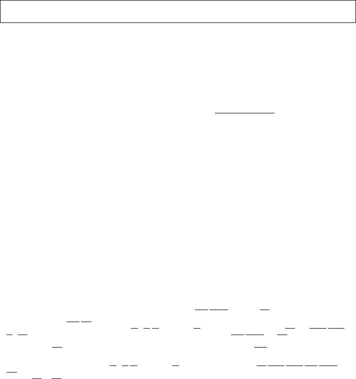
FUNCTIONAL BLOCK DIAGRAM
|
|
CS TIMEXP LINK 1 |
2–0 |
|
2,0 |
|
|
CS |
TIMEXP LINK 1 LINK 3 |
2–0 |
|
2,0 |
|
|
CPA |
LINK3 LINK4 IRQ |
FLAG |
LINK 0 |
LINK 0 |
LINK4 IRQ |
FLAG |
CPA |
|||||||
LINK 2 |
LINK 2 |
|||||||||||||
SPORT 1 |
|
|
|
LINK 5 |
LINK 5 |
|
|
|
SPORT 1 |
|||||
TDI |
|
SHARC_A |
|
SHARC_B |
TCK, TMS, TRST |
|
||||||||
|
|
TDO |
TDI |
|
|
|||||||||
|
LBOOT, BMS |
|
(ID2–0 = 1) |
|
|
|
EBOOT, LBOOT, BMS |
|
(ID2–0 = 2) |
|
|
|||
EBOOT, |
|
CLKIN RESET |
SPORT 0 |
|
1 3 |
|
CLKIN RESET |
SPORT 0 |
1 3 |
|||||
EMU |
TCK,TRSTTMS, FLAG FLAG |
EMU |
FLAG FLAG TDO |
|||||||||||
|
|
|
|
SHARC BUS (ADDR31–0, DATA47–0, MS3-0, RD, WR, PAGE, ADRCLK, |
||||||||||
|
|
|
|
SW, ACK, SBTS, HBR, HBG, REDY,, BR6–1, RPBA, DMAR1.2, DMAG1.2) |
||||||||||
EBOOT, |
|
|
CLKIN RESET |
SPORT0 |
|
1 3 |
EBOOT, LBOOT, BMS |
|
CLKIN RESET |
SPORT0 |
TCK,TMS,TRST |
1 3 |
||
LBOOT,BMS |
EMU |
SHARC_D |
TCK,TMS,TRST FLAG FLAG |
EMU |
SHARC_C |
FLAG FLAG TDI |
||||||||
(ID2–0 = 4) |
|
(ID2–0 |
= 3) |
|
||||||||||
CPA |
|
|
|
LINK 0 |
LINK 0 |
|
|
CPA |
||||||
SPORT 1 |
|
|
|
|
|
|
SPORT 1 |
|||||||
TDO |
|
|
|
0 |
LINK 2 |
LINK 2 |
|
|
0 |
|
||||
|
|
2–0 |
2, |
|
2–0 |
2, |
|
|||||||
|
|
|
|
LINK 5 |
LINK 5 |
|
|
|||||||
|
|
CS |
TIMEXP LINK1 |
LINK3 LINK4 IRQ FLAG |
TDI |
TDO |
CS |
TIMEXP LINK1 LINK3 LINK4 IRQ FLAG |
|
|||||
|
|
|
|
|
||||||||||
AD14060/AD14060L |
|
|
|
|
|
|
|
|
|
00667-001 |
||||
29 grams (typical) θJC = 0.36°C/W
GENERAL DESCRIPTION
The AD14060/AD14060L Quad-SHARC is the first in a family of high performance DSP multiprocessor modules. The core of the multiprocessor is the ADSP-21060 DSP microcomputer. The AD14060/AD14060L has the highest performance-to-density and lowest cost-to-performance ratios of any in its class. It is ideal for applications requiring higher levels of performance and/or functionality per unit area.
The AD14060/AD14060L takes advantage of the built-in multiprocessing features of the ADSP-21060 to achieve
480 peak MFLOPS with a single chip type in a single package. The on-chip SRAM of the DSPs provides 16 Mbits of onmodule shared SRAM. The complete shared bus (48 data,
Rev. B
Information furnished by Analog Devices is believed to be accurate and reliable. However, no responsibility is assumed by Analog Devices for its use, nor for any infringements of patents or other rights of third parties that may result from its use. Specifications subject to change without notice. No license is granted by implication or otherwise under any patent or patent rights of Analog Devices. Trademarks and registered trademarks are the property of their respective owners.
Figure 1.
32 address) is also brought off-module for interfacing with expansion memory or other peripherals.
The ADSP-21060 link ports are interconnected to provide direct communication among the four SHARCs, as well as high speed off-module access. Internally, each SHARC has a direct link port connection. Externally, each SHARC has a total of 120 Mbytes/s link port bandwidth.
Multiprocessor performance is enhanced with embedded power and ground planes, matched impedance interconnect, and optimized signal routing lengths and separation. The fully tested and ready-to-insert multiprocessor also significantly reduces board space.
One Technology Way, P.O. Box 9106, Norwood, MA 02062-9106, U.S.A. Tel: 781.329.4700 www.analog.com Fax: 781.326.8703 © 2004 Analog Devices, Inc. All rights reserved.

AD14060/AD14060L
TABLE OF CONTENTS |
|
Specifications..................................................................................... |
3 |
Electrical Characteristics (3.3 V, 5 V Supply)............................ |
3 |
Explanation of Test Levels........................................................... |
4 |
Timing Specifications....................................................................... |
5 |
Memory Read—Bus Master........................................................ |
8 |
Memory Write—Bus Master ....................................................... |
9 |
Synchronous Read/Write—Bus Master................................... |
10 |
Synchronous Read/Write—Bus Slave ...................................... |
12 |
Multiprocessor Bus Request and Host Bus Request .............. |
13 |
Asynchronous Read/Write—Host to AD14060/AD14060L. 15 |
|
Three-State Timing—Bus Master, Bus Slave, HBR, SBTS ..... 17 |
|
DMA Handshake........................................................................ |
18 |
Absolute Maximum Ratings.......................................................... |
27 |
ESD Caution................................................................................ |
27 |
Pin Configuration and Function Descriptions........................... |
28 |
Pin Function Descriptions ........................................................ |
30 |
Detailed Description ...................................................................... |
34 |
Architectural Features................................................................ |
34 |
Shared Memory Multiprocessing ............................................. |
34 |
Off-Module Memory and Peripherals Interface .................... |
36 |
REVISION HISTORY |
|
12/04—Rev. A to Rev. B |
|
Format Updated.................................................................. |
Universal |
Changes to Specifications Section.................................................. |
3 |
Changes to Development Tools Section ...................................... |
40 |
Changes to Target Board for Emulator Probe Section .............. |
40 |
Changes to Figure 27...................................................................... |
42 |
Updated Outline Dimensions ....................................................... |
48 |
Changes to Ordering Guide .......................................................... |
48 |
10/97—Rev. 0 to Rev. A |
|
4/97—Revision 0: Initial Version |
|
Link Port I/O............................................................................... |
38 |
Serial Ports .................................................................................. |
38 |
Program Booting........................................................................ |
38 |
Host Processor Interface ........................................................... |
39 |
Direct Memory Access (DMA) Controller ............................. |
39 |
Applications..................................................................................... |
40 |
Development Tools .................................................................... |
40 |
Quad-SHARC Development Board......................................... |
40 |
Other Package Details................................................................ |
40 |
Target Board Connector for Emulator Probe......................... |
40 |
Output Drive Currents .............................................................. |
42 |
Power Dissipation ...................................................................... |
42 |
Test Conditions........................................................................... |
43 |
Assembly Recommendations.................................................... |
45 |
PCB Layout Guidelines.............................................................. |
46 |
Mechanical Characteristics ....................................................... |
47 |
Additional Information ............................................................. |
47 |
Outline Dimensions ....................................................................... |
48 |
Ordering Guide .......................................................................... |
48 |
Rev. B | Page 2 of 48
AD14060/AD14060L
SPECIFICATIONS
Table 1. Recommended Operating Conditions
|
|
|
|
B Grade |
|
K Grade |
|
|
Parameter |
Min |
Max |
Min |
Max |
Unit |
|
|
VDD |
Supply Voltage (5 V) |
4.75 |
5.25 |
4.75 |
5.25 |
V |
|
|
Supply Voltage (3.3 V) |
3.15 |
3.6 |
3.15 |
3.6 |
V |
|
TCASE |
Case Operating Temperature |
−40 |
+100 |
0 |
+85 |
°C |
|
|
|
|
|
|
|
|
ELECTRICAL CHARACTERISTICS (3.3 V, 5 V SUPPLY)
Table 2.
|
|
|
|
|
Case |
Test |
|
|
|
|
|
|
5 V |
|
|
|
|
|
|
3.3 V |
|
|
|
||||||||
|
|
Parameter |
Temp |
Level |
Test Condition |
Min Typ |
Max |
Min |
Typ |
Max |
Unit |
||||||||||||||||||||
|
|
VIH1 |
High Level Input Voltage1 |
Full |
I |
@ VDD = max |
2.0 |
|
VDD + 0.5 |
2.0 |
|
|
|
|
VDD + 0.5 |
V |
|||||||||||||||
|
|
VIH2 |
High Level Input Voltage2 |
Full |
I |
@ VDD = max |
2.2 |
|
VDD + 0.5 |
2.2 |
|
|
|
|
VDD + 0.5 |
V |
|||||||||||||||
|
|
VIL |
Low Level Input Voltage1, 2 |
Full |
I |
@ VDD = min |
|
|
0.8 |
|
|
|
|
|
|
|
|
0.8 |
|
V |
|||||||||||
|
|
VOH |
High Level Output Voltage3, 4 |
Full |
I |
@ VDD = min, IOH = −2.0 mA |
4.1 |
|
|
|
|
2.4 |
|
|
|
|
|
|
V |
||||||||||||
|
|
VOL |
Low Level Output Voltage3, 4 |
Full |
I |
@ VDD = min, IOL = 4.0 mA |
|
|
0.4 |
|
|
|
|
|
|
|
|
0.4 |
|
V |
|||||||||||
|
|
IIH |
High Level Input Current5, 6, 7 |
Full |
I |
@ VDD = max, VIN = VDD max |
|
|
10 |
|
|
|
|
|
|
|
|
10 |
|
µA |
|||||||||||
|
|
IIL |
Low Level Input Current5 |
Full |
I |
@ VDD = max, VIN = 0 V |
|
|
10 |
|
|
|
|
|
|
|
|
10 |
|
µA |
|||||||||||
|
|
IILP |
Low Level Input Current6 |
Full |
I |
@ VDD = max, VIN = 0 V |
|
|
150 |
|
|
|
|
|
|
|
|
150 |
|
µA |
|||||||||||
|
|
IILPX4 |
Low Level Input Current7 |
Full |
I |
@ VDD = max, VIN = 0 V |
|
|
600 |
|
|
|
|
|
|
|
|
600 |
|
µA |
|||||||||||
|
|
IOZH |
Three-State Leakage Current8, 9, 10, 11 |
Full |
I |
@ VDD = max, VIN = VDD max |
|
|
10 |
|
|
|
|
|
|
|
|
10 |
|
µA |
|||||||||||
|
|
IOZL |
Three-State Leakage Current8, 12 |
Full |
I |
@ VDD = max, VIN = 0 V |
|
|
10 |
|
|
|
|
|
|
|
|
10 |
|
µA |
|||||||||||
|
|
IOZHP |
Three-State Leakage Current12 |
Full |
I |
@ VDD = max, VIN = VDD max |
|
|
350 |
|
|
|
|
|
|
|
|
350 |
|
µA |
|||||||||||
|
|
IOZLC |
Three-State Leakage Current13 |
Full |
I |
@ VDD = max, VIN = 0 V |
|
|
1.5 |
|
|
|
|
|
|
|
|
1.5 |
|
mA |
|||||||||||
|
|
IOZLA |
Three-State Leakage Current14 |
Full |
I |
@ VDD = max, |
|
|
350 |
|
|
|
|
|
|
|
|
350 |
|
µA |
|||||||||||
|
|
|
|
|
|
|
|
|
|
|
VIN = 1.5 V (5 V), 2 V (3.3 V) |
|
|
|
|
|
|
|
|
|
|
|
|
|
|
|
|||||
|
|
IOZLAR |
Three-State Leakage Current10 |
Full |
I |
@ VDD = max, VIN = 0 V |
|
|
4.2 |
|
|
|
|
|
|
|
|
4.2 |
|
mA |
|||||||||||
|
|
IOZLS |
Three-State Leakage Current9 |
Full |
I |
@ VDD = max, VIN = 0 V |
|
|
150 |
|
|
|
|
|
|
|
|
150 |
|
µA |
|||||||||||
|
|
IOZLSX4 |
Three-State Leakage Current11 |
Full |
I |
@ VDD = max, VIN = 0 V |
|
|
600 |
|
|
|
|
|
|
|
|
600 |
|
µA |
|||||||||||
|
|
IDDIN |
Supply Current (Internal)15 |
Full |
IV |
tCK = 25 ns, VDD = max |
1.4 |
|
2.92 |
|
|
|
|
1.0 |
|
2.2 |
|
A |
|||||||||||||
|
|
IDDIDLE |
Supply Current (Idle)16 |
Full |
I |
VDD = max |
|
|
800 |
|
|
|
|
|
|
|
|
760 |
|
mA |
|||||||||||
|
|
CIN |
Input Capacitance17, 18 |
25°C |
V |
|
|
|
|
|
|
15 |
|
|
|
|
|
|
|
15 |
|
|
|
|
pF |
||||||
|
|
|
|
|
|
|
|
|
|
|
|
|
|
|
|
|
|
|
|
|
|
|
|
|
|
|
|
|
|
|
|
|
|
|
|
|
|
|
|
|
|
|
|
|
|
|
|
|
|
|
|
|
|
|
|
|
|
|
|
|
|
|
|
1Applies to input and bidirectional pins: DATA47-0, ADDR31-0, RD, WR, SW, ACK, STBS, IRQy2-0, FLAGy0, FLAG1, FLAGy2, HBG, CSy, DMAR1, DMAR2, BR6-1, RPBA, CPAy, TFS0, TFSy1, RFS0, RFSy1, LyxDAT3-0, LyxCLK, LyxACK, EBOOTA, LBOOTA, EBOOTBCD, LBOOTBCD, BMSA, BMSBCD, TMS, TDI, TCK, HBR, DR0, DRy1, TCLK0, TCLKy1, RCLK0,
RCLKy1.
2 Applies to input pins: CLKIN, RESET, TRST.
3 Applies to output and bidirectional pins: DATA47-0, ADDR31-0, MS3-0, RD, WR, PAGE, ADRCLK, SW, ACK, FLAGy0, FLAG1, FLAGy2, TIMEXPy, HBG, REDY, DMAG1, DMAG2,
BR6-1, CPAy, DTO, DTy1, TCLK0, TCLKy1, RCLK0, RCLKy1, TFS0, TFSy1, RFS0, RFSy1, LyxDAT3-0, LyxCLK, LyxACK, BMSA, BMSBCD, TDO, EMU. 4 See the Output Drive Currents section for typical drive current capabilities.
5 Applies to input pins: STBS, IRQy2-0, HBR, CSy, DMAR1, DMAR2, RPBA, EBOOTA, LBOOTA, EBOOTBCD, LBOOTBCD, CLKIN, RESET, TCK. 6 Applies to input pins with internal pull-ups: DR0, DRy1, TDI.
7 Applies to bused input pins with internal pull-ups: TRST, TMS.
8Applies to three-statable pins: DATA47-0, ADDR31-0, MS3-0, RD, WR, PAGE, ADRCLK, SW, ACK, FLAGy0, FLAG1, FLAGy2, REDY, HBG, DMAG1, DMAG2, BMSA, BMSBCD, TDO, EMU. (Note that ACK is pulled up internally with 2 kΩ during reset in a multiprocessor system, when ID2-0 = 001 and another ADSP-2106x is not requesting bus
mastership. HBG and EMU are not tested for leakage current.)
9 Applies to three-statable pins with internal pull-ups: DTy1, TCLKy1, RCLKy1.
10Applies to ACK pin when pulled up. (Note that ACK is pulled up internally with 2 kΩ during reset in a multiprocessor system, when ID2-0 = 001 and another ADSP-2106x is not requesting bus mastership.)
11Applies to bused three-statable pins with internal pull-ups: DT0, TCLK0, RCLK0.
12Applies to three-statable pins with internal pull-downs: LyxDAT3-0, LyxCLK, LyxACK.
13Applies to CPAy pin.
14Applies to ACK pin, when the keeper latch is enabled.
15Applies to VDD pins. Conditions of operation: each processor is executing radix-2 FFT butterfly with instruction in cache, one data operand is fetched from each internal memory block, and one DMA transfer is occurring from/to internal memory at tCK = 25 ns.
16Applies to VDD pins. Idle denotes AD14060/AD14060L state during execution of IDLE instruction.
17Applies to all signal pins.
18Guaranteed, but not tested.
Rev. B | Page 3 of 48

AD14060/AD14060L
EXPLANATION OF TEST LEVELS
Test Level
I100% production tested.1
II100% production tested at 25°C, and sample tested at specified temperatures.
III Sample tested only.
IV Parameter is guaranteed by design and analysis, and characterization testing on discrete SHARCs.
VParameter is typical value only.
VI |
All devices are 100% production tested at 25°C, and |
|
sample tested at temperature extremes. |
1Link and serial ports: All are 100% tested at die level prior to assembly. All are 100% ac tested at module level; Link 4 and Serial 0 are also dc tested at the module level. See the Timing Specifications section.
Rev. B | Page 4 of 48
AD14060/AD14060L
TIMING SPECIFICATIONS
This data sheet represents production-released specifications for the AD14060 (5 V), and for the AD14060L (3.3 V). The ADSP-21060 die components are 100% tested, and the assembled AD14060/AD14060L units are again extensively tested at speed and across temperature. Parametric limits were established from the ADSP-21060 characterization followed by further design and analysis of the AD14060/AD14060L package characteristics.
The specifications are based on a CLKIN frequency of 40 MHz (tCK = 25 ns). The DT derating allows specifications at other CLKIN frequencies (within the minimum to maximum range of the tCK specification; see Table 3). DT is the difference between the actual CLKIN period and a CLKIN period of 25 ns:
DT = tCK − 25 ns
Use the exact timing information given. Do not attempt to derive parameters from the addition or subtraction of others. While addition or subtraction would yield meaningful results for an individual device, the values given in this data sheet
reflect statistical variations and worst cases. Consequently, one cannot meaningfully add parameters to derive longer times.
Switching Characteristics specify how the processor changes its signals. The user has no control over this timing—circuitry external to the processor must be designed for compatibility with these signal characteristics. Switching characteristics specify what the processor does in a given circumstance. The user can also use switching characteristics to ensure that any timing requirement of a device connected to the processor (such as memory) is satisfied.
Timing Requirements apply to signals that are controlled by circuitry external to the processor, such as the data input for a read operation. Timing requirements guarantee that the processor operates correctly with other devices.
(O/D) = Open Drain
(A/D) = Active Drive
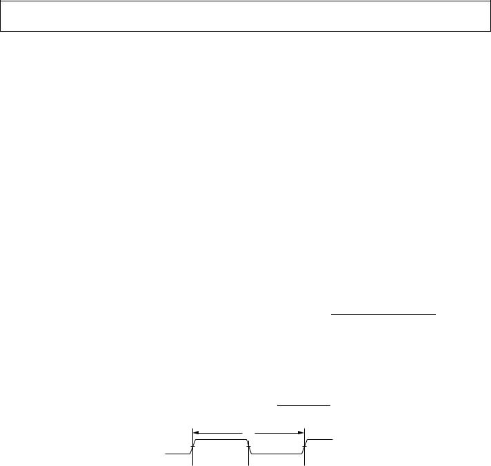
Table 3. Clock Input
|
|
|
|
40 MHz (5 V) |
|
40 MHz (3.3 V) |
|
|
|
Parameter |
Min |
|
Max |
Min |
Max |
Unit |
|
|
|
|
|
|
|
|
|
|
|
Clock Input |
|
|
|
|
|
|
|
|
Timing Requirements: |
|
|
|
|
|
|
|
|
tCK |
CLKIN Period |
25 |
100 |
25 |
100 |
ns |
|
|
tCKL |
CLKIN Width Low |
7 |
|
|
9.5 |
|
ns |
|
tCKH |
CLKIN Width High |
5 |
|
|
5 |
|
ns |
|
tCKRF |
CLKIN Rise/Fall (0.4 V to 2.0 V) |
|
3 |
|
3 |
ns |
|
|
|
|
|
|
|
|
|
|
tCK
CLKIN
 tCKH
tCKH 
 tCKL
tCKL 
00667-011
Figure 2. Clock Input
Rev. B | Page 5 of 48
AD14060/AD14060L
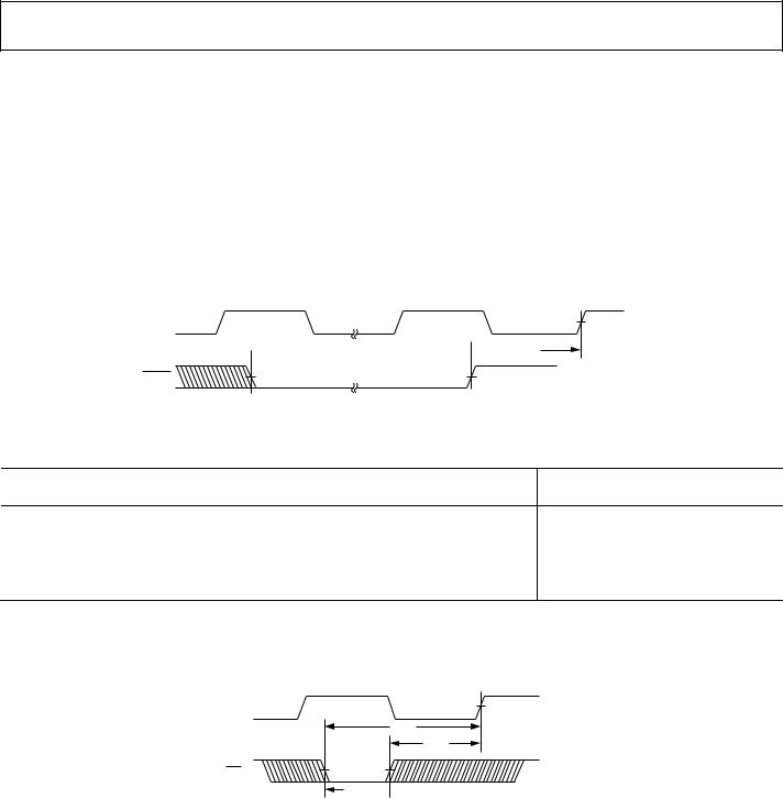
Table 4. Reset
|
|
|
|
|
|
|
5 V |
|
3.3 V |
|
|
|
|
|
Parameter |
Min |
Max |
Min |
Max |
Unit |
|||||
|
|
|
|
|
|
|
|
|
|
|
|
|
|
|
Reset |
|
|
|
|
|
|
|
|
|
|
|
|
Timing Requirements: |
|
|
|
|
|
|
|
|||
|
|
tWRST |
|
|
4 tCK |
|
4 tCK |
|
|
ns |
||
|
|
RESET |
Pulse Width Low1 |
|
|
|
||||||
|
|
tSRST |
|
|
14 + DT/2 |
tCK |
14 + DT/2 |
tCK |
ns |
|||
|
|
RESET |
Setup before CLKIN High2 |
|||||||||
|
|
|
|
|
|
|
|
|
|
|
|
|
|
|
|
|
|
|
|
|
|
|
|
|
|
1Applies after the power-up sequence is complete. At power-up, the processor’s internal phase-locked loop requires no more than 2000 CLKIN cycles while RESET is low, assuming stable VDD and CLKIN (not including start-up time of the external clock oscillator).
2Only required if multiple ADSP-2106xs must come out of reset synchronous to CLKIN with program counters (PC) equal (that is, for a SIMD system). Not required for multiple ADSP-2106xs communicating over the shared bus (through the external port), because the bus arbitration logic automatically synchronizes itself after reset.
CLKIN

 tWRST
tWRST 
 tSRST
tSRST
RESET
Figure 3. Reset
00667-012
Table 5. Interrupts
|
|
|
|
|
|
|
5 V |
Parameter |
Min |
Max |
|||||
Interrupts |
|
|
|
|
|
|
|
Timing Requirements: |
|
|
|||||
tSIR |
|
|
|
|
|
18 + 3 DT/4 |
|
IRQ2-0 Setup before CLKIN High1 |
|
||||||
tHIR |
|
|
|
|
|
|
11.5 + 3 DT/4 |
IRQ2-0 Hold before CLKIN High1 |
|
||||||
tIPW |
|
|
|
|
|
2 + tCK |
|
IRQ2-0 Pulse Width2 |
|
||||||
|
|
|
|
|
|
|
|
|
|
|
|
|
|
|
|
1 Only required for IRQx recognition in the following cycle. 2 Applies only if tSIR and tHIR requirements are not met.
CLKIN
tSIR
tHIR
IRQ2–0
tIPW 
Figure 4. Interrupts
|
3.3 V |
|
Min |
Max |
Unit |
18 + 3 DT/4 |
|
ns |
|
11.5 + 3 DT/4 |
ns |
2 + tCK |
|
ns |
|
|
|
00667-013
Rev. B | Page 6 of 48
AD14060/AD14060L
Table 6. Timer
|
|
|
|
5 V |
|
3.3 V |
|
|
Parameter |
|
Min |
Max |
Min |
Max |
Unit |
|
|
|
|
|
|
|
|
|
Timer |
|
|
|
|
|
|
|
Switching Characteristic: |
|
|
|
|
|
|
|
tDTEX |
CLKIN High to TIMEXP |
|
16 |
|
16 |
ns |
|
|
|
|
|
|
|
|
CLKIN
 tDTEX
tDTEX 
TIMEXP
 tDTEX
tDTEX 
00667-014
Figure 5. Timer
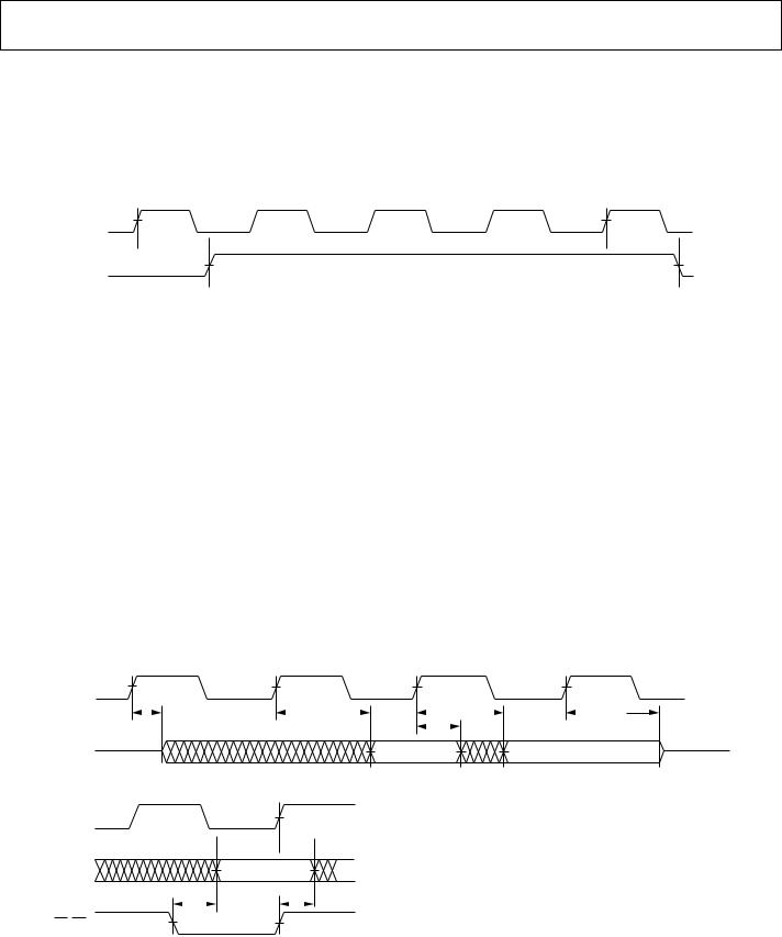
Table 7. Flags
|
|
|
|
|
|
|
|
|
|
|
|
5 V |
|
3.3 V |
|
|
|
Parameter |
Min |
Max |
Min |
Max |
Unit |
||||||||
|
|
Flags |
|
|
|
|
|
|
|
|
|
|
|
|
|
|
|
Timing Requirements: |
|
|
|
|
|
||||||||
|
|
tSFI |
FLAG2-0IN Setup before CLKIN High1 |
8 + 5 DT/16 |
|
8 + 5 DT/16 |
|
ns |
|||||||
|
|
tHFI |
FLAG2-0IN Hold after CLKIN High1 |
0.5 − 5 DT/16 |
|
0.5 − 5 DT/16 |
ns |
||||||||
|
|
tDWRFI |
FLAG2-0IN Delay after |
|
|
|
|
|
|
|
4.5 + 7 DT/16 |
|
4.5 + 7 DT/16 |
ns |
|
RD/WR Low1 |
|
|
|||||||||||||
|
|
tHFIWR |
FLAG2-0IN Hold after |
|
|
|
|
0.5 |
|
0.5 |
|
ns |
|||
RD/WR De-asserted1 |
|
|
|||||||||||||
|
|
Switching Characteristics: |
|
|
|
|
|
||||||||
|
|
tDFO |
FLAG2-0OUT Delay after CLKIN High |
|
17 |
|
17 |
ns |
|||||||
|
|
tHFO |
FLAG2-0OUT Hold after CLKIN High |
4 |
|
4 |
|
ns |
|||||||
|
|
tDFOE |
CLKIN High to FLAG2-0OUT Enable |
3 |
|
3 |
|
ns |
|||||||
|
|
tDFOD |
CLKIN High to FLAG2-0OUT Disable |
|
15 |
|
15 |
ns |
|||||||
|
|
|
|
|
|
|
|
|
|
|
|
|
|
|
|
|
|
|
|
|
|
|
|
|
|
|
|
|
|
|
|
1 Flag inputs that meet these setup and hold times affect conditional instructions in the following instruction cycle.
CLKIN
tDFOE |
|
|
|
|
|
|
|
|
|
||||
|
|
|
|
tDFO |
|
|
|
tDFO |
|
|
|
tDFOD |
|
|
|
|
|
|
|
|
|||||||
|
|
|
|
|
|
|
tHFO |
|
|
|
|
|
|
FLAG2–0OUT
FLAG OUTPUT
CLKIN
tHFI  tSFI
tSFI 


FLAG2–0IN
tDWRFI |
tHFIWR |
||
|
|
|
|
RD, WR
FLAG INPUT
00667-015
Figure 6. Flags
Rev. B | Page 7 of 48
AD14060/AD14060L
MEMORY READ—BUS MASTER
Use these specifications for asynchronous interfacing to memories (and memory-mapped peripherals) without reference to CLKIN. These specifications apply when the AD14060/AD14060L is the bus master accessing external memory space.
These switching characteristics also apply for bus master synchronous read/write timing (see the Synchronous Read/Write—Bus Master section). If these timing requirements are met, the synchronous read/write timing can be ignored (and vice versa).
Table 8. Specifications
|
|
|
|
|
|
|
|
|
|
|
|
|
|
|
|
|
|
5 V |
|
3.3 V |
|
|
Parameter |
Min |
Max |
Min |
Max |
Unit |
|||||||||||||||
|
|
|
|
|
|
|
|
|
|
|
|
|
|
|
|
|
|
|
|
|
|
|
Timing Requirements: |
|
|
|
|
|
|||||||||||||||
|
tDAD |
Address, Delay to Data Valid1, 2 |
|
17.5 + DT + W |
|
17.5 + DT + W |
ns |
||||||||||||||
|
tDRLD |
RD |
Low to Data Valid1 |
|
11.5 + 5 DT/8 + W |
|
11.5 + 5 DT/8 + W |
ns |
|||||||||||||
|
tHDA |
Data Hold from Address3 |
1 |
|
1 |
|
ns |
||||||||||||||
|
tHDRH |
Data Hold from |
RD |
|
High3 |
2.5 |
|
2.5 |
|
ns |
|||||||||||
|
tDAAK |
ACK Delay from Address2, 4 |
|
13.5 + 7 DT/8 + W |
|
13.5 + 7 DT/8 + W |
ns |
||||||||||||||
|
tDSAK |
ACK Delay from |
RD |
Low4 |
|
7.5 + DT/2 + W |
|
7.5 + DT/2 + W |
ns |
||||||||||||
|
Switching Characteristics: |
|
|
|
|
|
|||||||||||||||
|
tDRHA |
|
|
|
|
|
|
|
|
|
−0.5 + H |
|
−0.5 + H |
|
ns |
||||||
|
Address Hold after |
RD |
High |
|
|
||||||||||||||||
|
tDARL |
|
|
|
|
|
|
|
1.5 + 3 DT/8 |
|
1.5 + 3 DT/8 |
|
ns |
||||||||
|
Address to |
RD |
Low2 |
|
|
||||||||||||||||
|
tRW |
RD |
Pulse Width |
12.5 + 5 DT/8 + W |
12.5 + 5 DT/8 + W |
ns |
|||||||||||||||
|
tRWR |
|
|
|
|
|
|
Low |
8 + 3 DT/8 + HI |
|
8 + 3 DT/8 + HI |
|
ns |
||||||||
|
RD |
High to |
WR, |
|
RD, |
|
DMAGx |
|
|
||||||||||||
|
tSADADC |
Address Setup before ADRCLK High2 |
−0.5 + DT/4 |
|
−0.5 + DT/4 |
|
ns |
||||||||||||||
W = number of wait states specified in WAIT register × tCK.
HI = tCK, if an address hold cycle or bus idle cycle occurs, as specified in WAIT register; otherwise, HI = 0.
H = tCK, if an address hold cycle occurs as specified in WAIT register; otherwise, H = 0.
1 Data delay/setup: User must meet tDAD, tDRLD, or synchronous specification, tSSDATI.
2 For MSx, SW, BMS, the falling edge is referenced.
3Data hold: User must meet tHDA, tHDRH, or synchronous specification, tHDATI. See the System Hold Time Calculation Example section for the calculation of hold times given capacitive and dc loads.
4 ACK delay/setup: User must meet tDSAK, tDAAK, or synchronous specification, tSACKC.
ADDRESS |
|
|
MSx, SW |
|
|
BMS |
tDARL |
tDRHA |
|
||
|
|
tRW |
RD |
|
|
|
|
tHDA |
|
|
tDRLD |
|
tDAD |
tHDRH |
DATA |
tDSAK |
|
|
tRWR |
|
|
tDAAK |
|
ACK |
|
|
WR, DMAG |
tSADADC |
|
ADRCLK |
|
00667-016 |
(OUT) |
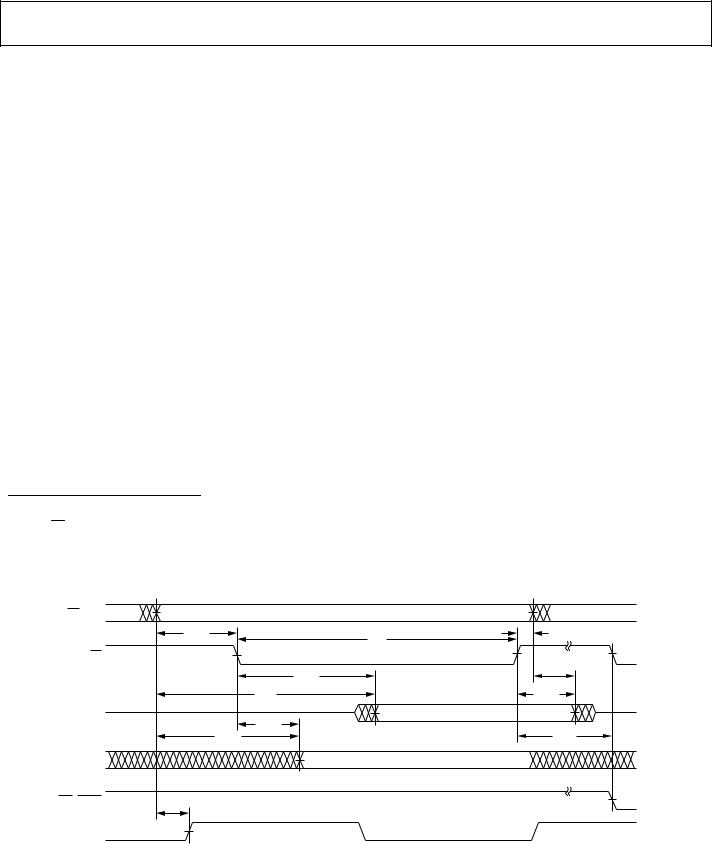
|
Figure 7. Memory Read—Bus Master
Rev. B | Page 8 of 48
AD14060/AD14060L
MEMORY WRITE—BUS MASTER
Use these specifications for asynchronous interfacing to memories (and memory-mapped peripherals) without reference to CLKIN. These specifications apply when the AD14060/AD14060L is the bus master accessing external memory space.
These switching characteristics also apply for bus master synchronous read/write timing (see the Synchronous Read/Write—Bus Master section). If these timing requirements are met, the synchronous read/write timing can be ignored (and vice versa).
Table 9. Specifications
|
|
|
|
|
|
|
|
|
|
|
|
|
|
|
|
|
|
|
|
|
|
|
|
5 V |
|
3.3 V |
|
|
|
Parameter |
Min |
Max |
Min |
Max |
Unit |
||||||||||||||||||||||
|
|
|
|
|
|
|
|
|
|
|
|
|
|
|
|
|
|
|
|
|
|
|
|
|
|
|
|
|
|
Timing Requirements: |
|
|
|
|
|
||||||||||||||||||||||
|
tDAAK |
ACK Delay from Address, Selects1, 2 |
|
13.5 + 7 DT/8 + W |
|
13.5 + 7 DT/8 + W |
ns |
|||||||||||||||||||||
|
tDSAK |
ACK Delay from |
WR |
Low1 |
|
8 + DT/2 + W |
|
8 + DT/2 + W |
ns |
|||||||||||||||||||
|
Switching Characteristics: |
|
|
|
|
|
||||||||||||||||||||||
|
tDAWH |
|
|
|
|
|
|
|
|
|
|
|
|
|
|
|
|
|
|
16.5 + 15 DT/16 + W |
|
16.5 + 15 DT/16 + W |
|
ns |
||||
|
Address, Selects to |
WR |
|
|
|
|
|
|
|
|||||||||||||||||||
|
|
De-asserted2 |
|
|
|
|
|
|||||||||||||||||||||
|
tDAWL |
Address, Selects to |
WR |
Low2 |
2.5 + 3 DT/8 |
|
2.5 + 3 DT/8 |
|
ns |
|||||||||||||||||||
|
tWW |
WR |
Pulse Width |
12 + 9 DT/16 + W |
|
12 + 9 DT/16 + W |
|
ns |
||||||||||||||||||||
|
tDDWH |
|
|
|
|
|
|
|
|
|
|
|
|
|
|
|
6.5 + DT/2 + W |
|
6.5 + DT/2 + W |
|
ns |
|||||||
|
Data Setup before |
WR |
|
High |
|
|
||||||||||||||||||||||
|
tDWHA |
|
|
|
|
|
|
|
|
|
|
|
|
|
0 + DT/16 + H |
|
0 + DT/16 + H |
|
ns |
|||||||||
|
Address Hold after |
WR |
De-asserted |
|
|
|||||||||||||||||||||||
|
tDATRWH |
|
|
|
|
|
|
|
|
|
|
|
0.5 + DT/16 + H |
6.5 + DT/16 + H |
0.5 + DT/16 + H |
6.5 + DT/16 + H |
ns |
|||||||||||
|
Data Disable after |
WR |
De-asserted3 |
|||||||||||||||||||||||||
|
tWWR |
WR |
High to |
WR, |
|
RD, |
|
DMAGx |
|
Low |
8 + 7 DT/16 + H |
|
8 + 7 DT/16 + H |
|
ns |
|||||||||||||
|
tDDWR |
|
|
|
4.5 + 3 DT/8 + 1 |
|
4.5 + 3 DT/8 + 1 |
|
ns |
|||||||||||||||||||
|
Data Disable before |
WR |
or |
RD |
Low |
|
|
|||||||||||||||||||||
|
tWDE |
|
−1.5 + DT/16 |
|
−1.5 + DT/16 |
|
ns |
|||||||||||||||||||||
|
WR |
Low to Data Enabled |
|
|
||||||||||||||||||||||||
|
tSADADC |
Address, Selects to ADRCLK High2 |
−0.5 + DT/4 |
|
−0.5 + DT/4 |
|
ns |
|||||||||||||||||||||
W = number of wait states specified in WAIT register × tCK.
H = tCK, if an address hold cycle occurs, as specified in WAIT register; otherwise, H = 0.
I = tCK, if a bus idle cycle occurs, as specified in WAIT register; otherwise, I = 0.
1 ACK delay/setup: User must meet tDAAK, tDSAK, or synchronous specification, tSACKC.
2 For MSx, SW, BMS, the falling edge is referenced.
3 See the System Hold Time Calculation Example section for the calculation of hold times given capacitive and dc loads.
ADDRESS |
|
|
|
MSx, SW |
|
|
|
BMS |
|
|
|
|
tDAWH |
|
tDWHA |
|
tDAWL |
tWW |
|
WR |
|
|
|
|
tWDE |
tDDWH |
tWWR |
|
tDDWR |
||
|
|
|
tDATRWH |
DATA |
|
|
|
|
tDSAK |
|
|
|
tDAAK |
|
|
ACK |
|
|
|
RD, DMAG |
tSADADC |
|
|
|
|
|
|
ADRCLK |
|
|
017 |
|
|
00667- |
|
(OUT) |
|
|
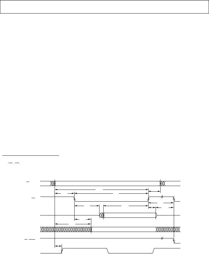
Figure 8. Memory Write—Bus Master
Rev. B | Page 9 of 48

AD14060/AD14060L
SYNCHRONOUS READ/WRITE—BUS MASTER
Use these specifications for interfacing to external memory systems that require CLKIN—relative timing or for accessing a slave
ADSP 2106x in multiprocessor memory space. These synchronous switching characteristics are also valid during asynchronous memory reads and writes (see the Memory Read—Bus Master and Memory Write—Bus Master sections).
When accessing a slave ADSP-2106x, these switching characteristics must meet the slave’s timing requirements for synchronous read/writes (see the Synchronous Read/Write—Bus Slave section). The slave ADSP-2106x must also meet these bus master timing requirements for data and acknowledge setup and hold times.
Table 10. Specifications
|
|
|
|
|
|
|
|
|
|
|
|
|
|
|
|
|
|
|
|
5 V |
|
3.3 V |
|
|
Parameter |
Min |
Max |
Min |
Max |
Unit |
|||||||||||||||||
|
Timing Requirements: |
|
|
|
|
|
|||||||||||||||||
|
tSSDATI |
Data Setup before CLKIN |
3 + DT/8 |
|
3 + DT/8 |
|
ns |
||||||||||||||||
|
tHSDATI |
Data Hold after CLKIN |
4 − DT/8 |
|
4 − DT/8 |
|
ns |
||||||||||||||||
|
tDAAK |
|
|
|
|
|
|
|
|
|
|
|
|
|
|
|
|
|
|
13.5 + 7 DT/8 + W |
|
13.5 + 7 DT/8 + W |
ns |
|
ACK Delay after Address, |
MSx, SW, BMS1, 2 |
|
|
|||||||||||||||||||
|
tSACKC |
ACK Setup before CLKIN2 |
6.5 + DT/4 |
|
6.5 + DT/4 |
|
ns |
||||||||||||||||
|
tHACKC |
ACK Hold after CLKIN |
−0.5 − DT/4 |
|
−0.5 − DT/4 |
|
ns |
||||||||||||||||
|
Switching Characteristics: |
|
|
|
|
|
|||||||||||||||||
|
tDADRO |
|
|
|
|
|
|
|
|
|
|
|
|
8 − DT/8 |
|
8 − DT/8 |
ns |
||||||
|
Address, |
MSx, BMS, SW, Delay after CLKIN1 |
|
|
|||||||||||||||||||
|
tHADRO |
Address, |
|
|
|
|
|
|
−1 − DT/8 |
|
−1 − DT/8 |
|
ns |
||||||||||
MSx, BMS, SW, Hold after CLKIN |
|
|
|||||||||||||||||||||
|
tDPGC |
PAGE Delay after CLKIN |
9 + DT/8 |
17 + DT/8 |
9 + DT/8 |
17 + DT/8 |
ns |
||||||||||||||||
|
tDRDO |
|
High Delay after CLKIN |
−2 − DT/8 |
+5 − DT/8 |
−2 − DT/8 |
+5 − DT/8 |
ns |
|||||||||||||||
|
RD |
|
|||||||||||||||||||||
|
tDWRO |
|
High Delay after CLKIN |
−3 − 3 DT/16 |
+5 − 3 DT/16 |
−3 − 3 DT/16 |
+5 − 3 DT/16 |
ns |
|||||||||||||||
|
WR |
|
|||||||||||||||||||||
|
tDRWL |
|
|
|
|
8 + DT/4 |
13.5 + DT/4 |
8 + DT/4 |
13.5 + DT/4 |
ns |
|||||||||||||
|
RD/WR Low Delay after CLKIN |
||||||||||||||||||||||
|
tSDDATO |
Data Delay after CLKIN |
|
20 + 5 DT/16 |
|
20.25 + 5 DT/16 |
ns |
||||||||||||||||
|
tDATTR |
Data Disable after CLKIN3 |
0 − DT/8 |
8 − DT/8 |
0 − DT/8 |
8 – DT/8 |
ns |
||||||||||||||||
|
tDADCCK |
ADRCLK Delay after CLKIN |
4 + DT/8 |
11 + DT/8 |
4 + DT/8 |
11 + DT/8 |
ns |
||||||||||||||||
|
tADRCK |
ADRCLK Period |
tCK |
|
tCK |
|
ns |
||||||||||||||||
|
tADRCKH |
ADRCLK Width High |
(tCK/2 − 2) |
|
(tCK/2 − 2) |
|
ns |
||||||||||||||||
|
tADRCKL |
ADRCLK Width Low |
(tCK/2 − 2) |
|
(tCK/2 − 2) |
|
ns |
||||||||||||||||
W = number of wait states specified in WAIT register × tCK.
1 For MSx, SW, BMS, the falling edge is referenced.
2 ACK delay/setup: User must meet tDAAK, tDSAK, or synchronous specification, tSACKC.
3 See the System Hold Time Calculation Example section for the calculation of hold times given capacitive and dc loads.
Rev. B | Page 10 of 48
AD14060/AD14060L
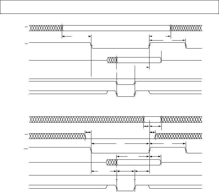
CLKIN |
|
|
|
tADRCK |
|
tDADCCK |
tADRCKH |
tADRCKL |
ADRCLK |
|
|
tDADRO |
tDAAK |
tHADRO |
|
||
ADDRESS |
|
|
SW |
|
|
|
tDPGC |
|
PAGE |
|
|
|
tSACKC |
tHACKC |
|
|
|
ACK |
|
|
(IN) |
|
|
READ CYCLE |
|
|
|
tDRWL |
tDRDO |
RD |
|
|
|
tSSDATI |
tHSDATI |
DATA |
|
|
(IN) |
|
|
WRITE CYCLE |
tDRWL |
tDWRO |
|
||
|
|
|
WR |
|
|
|
tSDDATO |
tDATTR |
DATA (OUT)
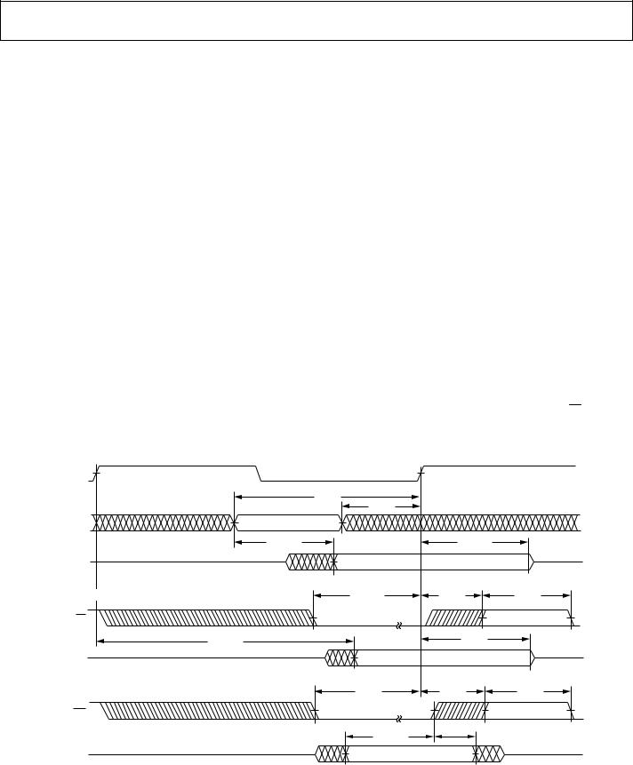
Figure 9. Synchronous Read/Write—Bus Master
00667-018
Rev. B | Page 11 of 48
AD14060/AD14060L
SYNCHRONOUS READ/WRITE—BUS SLAVE
Use these specifications for bus master access to a slave’s IOP registers or internal memory in multiprocessor memory space. The bus master must meet these bus slave timing requirements.
Table 11. Specifications
|
|
|
|
|
|
|
|
|
|
|
|
|
|
|
|
|
|
5 V |
3.3 V |
|
|
|
|
Parameter |
Min |
Max |
Min |
Max |
Unit |
||||||||||||||
|
|
|
|
|
|
|
|
|
|
|
|
|
|
|
|
|
|
|
|
|
|
|
|
Timing Requirements: |
|
|
|
|
|
||||||||||||||
|
|
tSADRI |
|
|
|
|
|
|
|
|
|
|
|
|
15.5 + DT/2 |
|
15.5 + DT/2 |
|
ns |
||
|
|
Address, |
SW |
Setup before CLKIN |
|
|
|||||||||||||||
|
|
tHADRI |
|
|
|
|
|
|
|
|
|
|
|
|
|
4.5 + DT/2 |
|
4.5 + DT/2 |
ns |
||
|
|
Address, |
SW |
Hold before CLKIN |
|
|
|||||||||||||||
|
|
tSRWLI |
|
|
|
|
|
|
|
|
|
|
|
|
9.5 + 5 DT/16 |
|
9.5 + 5 DT/16 |
|
ns |
||
|
|
|
RD/WR Low Setup before CLKIN1 |
|
|
||||||||||||||||
|
|
tHRWLI |
|
|
|
|
|
|
|
|
|
|
|
−3.5 − 5 DT/16 |
+8 + 7 DT/16 |
−3.25 − 5 DT/16 |
+8 + 7 DT/16 |
ns |
|||
RD/WR Low Hold after CLKIN |
|||||||||||||||||||||
|
|
tRWHPI |
|
|
|
|
|
|
|
|
|
|
|
3 |
|
3 |
|
ns |
|||
|
|
RD/WR Pulse High |
|
|
|||||||||||||||||
|
|
tSDATWH |
|
|
|
|
|
|
5.5 |
|
5.5 |
|
ns |
||||||||
|
|
Data Setup before |
WR |
High |
|
|
|||||||||||||||
|
|
tHDATWH |
|
|
|
|
1.5 |
|
1.5 |
|
ns |
||||||||||
|
|
Data Hold after |
WR |
High |
|
|
|||||||||||||||
|
|
Switching Characteristics: |
|
|
|
|
|
||||||||||||||
|
|
tSDDATO |
Data Delay after CLKIN |
|
20 + 5 DT/16 |
|
20.25 + 5 DT/16 |
ns |
|||||||||||||
|
|
tDATTR |
Data Disable after CLKIN2 |
0 − DT/8 |
8 − DT/8 |
0 − DT/8 |
8 − DT/8 |
ns |
|||||||||||||
|
|
tDACKAD |
ACK Delay after Address, |
SW |
3 |
|
10 |
|
10 |
ns |
|||||||||||
|
|
tACKTR |
ACK Disable after CLKIN3 |
−1 − DT/8 |
+7 − DT/8 |
−1 − DT/8 |
+7 − DT/8 |
ns |
|||||||||||||
|
|
|
|
|
|
|
|
|
|
|
|
|
|
|
|
|
|
|
|
|
|
1tSRWLI (min) = 9.5 + 5 DT/16 when the multiprocessor memory space wait state (MMSWS bit in WAIT register) is disabled; when MMSWS is enabled, tSRWLI (min) = 4 + DT/8.
2 See the System Hold Time Calculation Example section for the calculation of hold times given capacitive and dc loads.
3tDACKAD is true only if the address and SW inputs have setup times (before CLKIN) greater than 10.5 + DT/8 and less than 18.5 + 3 DT/4. If the address and SW inputs have setup times greater than 19 + 3 DT/4, then ACK is valid 15 + DT/4 (max) after CLKIN. A slave that sees an address with an M field match responds with ACK regardless of the state of MMSWS or strobes. A slave three-states ACK every cycle with tACKTR.
CLKIN |
|
|
|
|
tSADRI |
|
|
ADDRESS |
tHADRI |
|
|
|
|
|
|
SW |
|
|
|
|
tDACKAD |
tACKTR |
|
ACK |
|
|
|
READ ACCESS |
tSRWLI |
tHRWLI |
tRWHPI |
RD |
|
|
|
|
tSDDATO |
tDATTR |
|
DATA |
|
|
|
(OUT) |
|
|
|
WRITE ACCESS |
tSRWLI |
tHRWLI |
tRWHPI |
|
|||
WR |
|
|
|
|
tSDATWH |
tHDATWH |
|
|
|
|
DATA (IN)
00667-019
Figure 10. Synchronous Read/Write—Bus Slave
Rev. B | Page 12 of 48

AD14060/AD14060L
MULTIPROCESSOR BUS REQUEST AND HOST BUS REQUEST
Use these specifications for passing of the bus mastership among multiprocessing ADSP-2106xs (BRx) or a host processor (HBR, HBG).
Table 12. Specifications
|
|
|
|
|
|
|
|
|
|
|
|
|
|
|
|
|
|
|
|
|
|
|
|
|
|
|
|
|
|
|
|
5 V |
|
|
|
|
|
|
|
3.3 V |
|
|
|
Parameter |
Min |
Max |
Min |
Max |
Unit |
||||||||||||||||||||||||||||||||||
|
|
|
|
|
|
|
|
|
|
|
|
|
|
|
|
|
|
|
|
|
|
|
|
|
|
|
|
|
|
|
|
|
|
|
|
|
|
|
|
|
|
|
|
Timing Requirements: |
|
|
|
|
|
|
|
|
|
|
|
||||||||||||||||||||||||||||
|
|
tHBGRCSV |
|
|
|
|
|
Low to |
|
|
|
|
|
|
|
|
|
|
|
|
|
|
|
|
|
|
|
|
|
|
|
19.5 + 5 DT/4 |
|
|
19.5 + 5 DT/4 |
ns |
|||||
|
|
HBG |
|
RD/WR/CS Valid1 |
|
|
|
|
|||||||||||||||||||||||||||||||||
|
|
tSHBRI |
HBR |
Setup before CLKIN2 |
20 |
+ 3 DT/4 |
|
|
|
|
|
20 |
+ 3 DT/4 |
|
ns |
||||||||||||||||||||||||||
|
|
tHHBRI |
|
|
|
|
|
|
|
|
|
|
|
|
|
|
|
|
|
|
|
|
|
|
13.5 + 3 DT/4 |
|
|
13.5 + 3 DT/4 |
ns |
||||||||||||
|
|
HBR |
Hold before CLKIN2 |
|
|
|
|
||||||||||||||||||||||||||||||||||
|
|
tSHBGI |
HBG |
|
Setup before CLKIN |
13 |
+ DT/2 |
|
|
|
|
|
13 |
+ DT/2 |
|
ns |
|||||||||||||||||||||||||
|
|
tHHBGI |
|
|
|
Hold before CLKIN High |
|
|
5.5 + DT/2 |
|
|
5.5 + DT/2 |
ns |
||||||||||||||||||||||||||||
|
|
HBG |
|
|
|
|
|
||||||||||||||||||||||||||||||||||
|
|
tSBRI |
|
|
|
|
|
|
|
|
|
|
|
|
|
|
|
|
|
|
|
|
13 |
+ DT/2 |
|
|
|
|
|
13 |
+ DT/2 |
|
ns |
||||||||
|
|
BRx, CPA Setup before CLKIN3 |
|
|
|
|
|
|
|||||||||||||||||||||||||||||||||
|
|
tHBRI |
|
|
|
|
|
|
|
|
|
|
|
|
|
|
|
|
|
|
|
|
|
|
5.5 + DT/2 |
|
|
5.5 + DT/2 |
ns |
||||||||||||
BRx, CPA Hold before CLKIN High |
|
|
|
|
|||||||||||||||||||||||||||||||||||||
|
|
tSRPBAI |
RPBA Setup before CLKIN |
21 |
+ 3 DT/4 |
|
|
|
|
|
21 |
+ 3 DT/4 |
|
ns |
|||||||||||||||||||||||||||
|
|
tHRPBAI |
RPBA Hold before CLKIN |
|
|
11.5 + 3 DT/4 |
|
|
11.5 + 3 DT/4 |
ns |
|||||||||||||||||||||||||||||||
|
|
Switching Characteristics: |
|
|
|
|
|
|
|
|
|
|
|
||||||||||||||||||||||||||||
|
|
tDHBGO |
|
|
|
|
|
|
|
|
|
|
|
|
|
|
|
|
|
|
|
8 − DT/8 |
|
|
8 − DT/8 |
ns |
|||||||||||||||
|
|
HBG |
Delay after CLKIN |
|
|
|
|
||||||||||||||||||||||||||||||||||
|
|
tHHBGO |
|
|
|
|
|
|
|
|
|
|
|
|
|
|
|
|
|
−2 − DT/8 |
|
|
|
|
|
−2 − DT/8 |
|
ns |
|||||||||||||
|
|
HBG |
Hold after CLKIN |
|
|
|
|
|
|
||||||||||||||||||||||||||||||||
|
|
tDBRO |
|
|
|
|
|
|
|
|
|
|
|
|
|
|
|
|
|
|
|
|
8 − DT/8 |
|
|
8 − DT/8 |
ns |
||||||||||||||
|
|
BRx Delay after CLKIN |
|
|
|
|
|||||||||||||||||||||||||||||||||||
|
|
tHBRO |
|
|
|
|
|
|
|
|
|
|
|
|
|
|
|
|
|
|
−2 − DT/8 |
|
|
|
|
|
−2 − DT/8 |
|
ns |
||||||||||||
|
|
BRx Hold after CLKIN |
|
|
|
|
|
|
|||||||||||||||||||||||||||||||||
|
|
tDCPAO |
|
|
|
|
|
|
|
|
|
|
|
|
|
|
|
|
|
|
9 − DT/8 |
|
|
9.5 − DT/8 |
ns |
||||||||||||||||
|
|
CPA |
Low Delay after CLKIN |
|
|
|
|
||||||||||||||||||||||||||||||||||
|
|
tTRCPA |
|
|
|
|
|
|
|
|
|
|
|
|
|
|
|
|
–2 − DT/8 |
+5.5 − DT/8 |
−2 − DT/8 |
+5.5 − DT/8 |
ns |
||||||||||||||||||
|
|
CPA |
Disable after CLKIN |
||||||||||||||||||||||||||||||||||||||
|
|
tDRDYCS |
|
|
|
|
|
|
|
|
|
|
|
Low4 |
|
|
9.5 |
|
|
|
|
|
|
12 |
ns |
||||||||||||||||
|
|
REDY (O/D) or (A/D) Low from |
CS |
and |
HBR |
|
|
|
|
|
|
|
|
||||||||||||||||||||||||||||
|
|
tTRDYHG |
REDY (O/D) Disable or REDY (A/D) High from |
HBG |
4 |
40 |
+ 27 DT/16 |
|
|
|
|
|
40 |
+ 27 DT/16 |
ns |
||||||||||||||||||||||||||
|
|
tARDYTR |
|
|
|
|
|
|
|
High4 |
|
|
11 |
|
|
|
|
|
|
11 |
ns |
||||||||||||||||||||
|
|
REDY (A/D) Disable from |
CS |
or |
HBR |
|
|
|
|
|
|
|
|
||||||||||||||||||||||||||||
|
|
|
|
|
|
|
|
|
|
|
|
|
|
|
|
|
|
|
|
|
|
|
|
|
|
|
|
|
|
|
|
|
|
|
|
|
|
|
|
|
|
|
|
|
|
|
|
|
|
|
|
|
|
|
|
|
|
|
|
|
|
|
|
|
|
|
|
|
|
|
|
|
|
|
|
|
|
|
|
|
|
|
|
1For first asynchronous access after HBR and CS asserted, ADDR31–0 must be a non-MMS value 1/2 tCK before RD or WR goes low, or by tHBGRCSV after HBG goes low. This is easily accomplished by driving an upper address signal high when HBG is asserted.
2 Required only for recognition in the current cycle.
3 CPA assertion must meet the setup to CLKIN; de-assertion does not need to meet the setup to CLKIN. 4 (O/D) = open drain; (A/D) = active drive.
Rev. B | Page 13 of 48

AD14060/AD14060L
CLKIN |
|
|
tSHBRI |
tHHBRI |
|
|
|
|
HBR |
|
|
|
tDHBGO |
|
HBG |
tHHBGO |
|
|
|
|
(OUT) |
|
|
|
tDBRO |
|
|
tHBRO |
|
BRx |
|
|
(OUT) |
|
|
CPA (OUT) |
tDCPAO |
tTRCPA |
(O/D) |
|
|
|
|
tSHBGI |
|
|
tHHBGI |
HBG (IN) |
|
|
|
|
tSBRI |
BRx (IN) |
|
tHBRI |
|
|
|
CPA (IN) (O/D) |
|
|
HBR |
|
|
CS |
|
|
tDRDYCS |
tTRDYHG |
|
REDY (O/D)
tARDYTR
REDY (A/D)
tHBGRCSV
HBG (OUT)
RD
WR
CS |
|
tSRPBAI |
|
 tHRPBAI
RPBA
O/D = OPEN DRAIN, A/D = ACTIVE DRIVE
HBG IS DELAYED BY n CLOCK CYCLES WHEN WAIT STATES OR BUS LOCK ARE IN EFFECT.
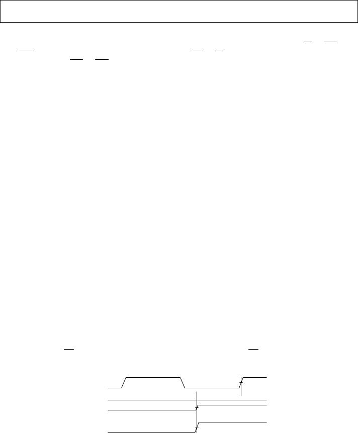
Figure 11. Multiprocessor Bus Request and Host Bus Request
00667-020
Rev. B | Page 14 of 48
AD14060/AD14060L
ASYNCHRONOUS READ/WRITE—HOST TO AD14060/AD14060L
Use these specifications for asynchronous host processor access to an AD14060/AD14060L, after the host has asserted CS and HBR (low).
After HBG is returned by the AD14060/AD14060L, the host can drive the RD and WR pins to access the AD14060/AD14060L’s internal
memory or IOP registers. HBR and HBG are assumed low for this timing.
Table 13. Specifications
|
|
|
|
|
|
|
|
|
|
|
|
|
|
|
|
|
|
|
|
|
|
|
|
|
|
|
|
|
|
|
|
|
|
|
|
|
|
|
|
|
|
5 V |
|
3.3 V |
|
|
|
|
||
|
|
Parameter |
|
|
|
|
|
|
|
|
|
|
|
|
|
|
|
|
|
|
|
|
|
|
|
|
|
|
|
|
|
|
|
|
|
|
|
|
|
Min |
Max |
Min |
|
Max |
Unit |
|||||
|
|
|
|
|
|
|
|
|
|
|
|
|
|
|
|
|
|
|
|
|
|
|
|
|
|
|
|
|
|
|
|
|
|
|
|
|
|
|
|
|
|
|
|
|
|
|
|
|
|
|
|
|
Read Cycle |
|
|
|
|
|
|
|
|
|
|
|
|
|
|
|
|
|
|
|
|
|
|
|
|
|
|
|
|
|
|
|
|
|
|
|
|
|
|
|
|
|
|
|
|
|
|
|
|
|
|
Timing Requirements: |
|
|
|
|
|
|
|
|
|
|
|
|||||||||||||||||||||||||||||||||||||
|
|
tSADRDL |
|
|
|
|
|
|
|
|
|
|
|
|
|
|
|
|
|
|
|
|
|
|
|
|
|
|
|
|
|
|
|
|
|
|
|
|
|
0.5 |
|
|
0.5 |
|
|
|
ns |
|||
|
|
Address Setup/CS |
|
|
Low before RD Low1 |
|
|
|
|
|
||||||||||||||||||||||||||||||||||||||||
|
|
tHADRDH |
|
|
|
|
|
|
|
|
|
|
|
|
|
|
|
|
|
|
|
|
|
|
|
|
|
|
|
|
|
|
|
|
|
0.5 |
|
|
0.5 |
|
|
|
ns |
|||||||
|
|
Address Hold/CS |
Hold Low after |
RD |
|
|
|
|
|
|
|
|
|
|
|
|
|
|||||||||||||||||||||||||||||||||
|
|
tWRWH |
|
|
|
|
|
|
|
|
|
|
|
|
|
|
|
|
|
|
|
|
|
|
|
|
|
|
|
|
|
6 |
|
|
6 |
|
|
|
ns |
|||||||||||
|
|
RD/WR High Width |
|
|
|
|
|
|||||||||||||||||||||||||||||||||||||||||||
|
|
tDRDHRDY |
|
|
|
High Delay after REDY (O/D) Disable |
0 |
|
|
0 |
|
|
|
ns |
||||||||||||||||||||||||||||||||||||
|
|
RD |
|
|
|
|
|
|
||||||||||||||||||||||||||||||||||||||||||
|
|
tDRDHRDY |
|
|
|
High Delay after REDY (A/D) Disable |
0 |
|
|
0 |
|
|
|
ns |
||||||||||||||||||||||||||||||||||||
|
|
RD |
|
|
|
|
|
|
||||||||||||||||||||||||||||||||||||||||||
|
|
Switching Characteristics: |
|
|
|
|
|
|
|
|
|
|
|
|||||||||||||||||||||||||||||||||||||
|
|
tSDATRDY |
Data Valid before REDY Disable from Low |
1.5 |
|
|
1.5 |
|
|
|
ns |
|||||||||||||||||||||||||||||||||||||||
|
|
tDRDYRDL |
|
|
|
|
|
|
|
|
|
|
|
|
|
|
|
|
|
|
|
|
|
|
|
|
|
|
11 |
|
13.5 |
|
ns |
|||||||||||||||||
|
|
REDY (O/D) or (A/D) Low Delay after |
RD |
|
Low |
|
|
|
|
|||||||||||||||||||||||||||||||||||||||||
|
|
tRDYPRD |
REDY (O/D) or (A/D) Low Pulse Width for Read |
45 + DT |
|
45 + DT |
|
|
|
ns |
||||||||||||||||||||||||||||||||||||||||
|
|
tHDARWH |
|
|
|
|
|
|
|
|
|
|
|
|
|
|
|
|
|
|
|
|
|
|
1.5 |
|
9 |
1.5 |
9.5 |
|
ns |
|||||||||||||||||||
|
|
Data Disable after |
RD |
|
|
High |
|
|
||||||||||||||||||||||||||||||||||||||||||
|
|
|
|
|
|
|
|
|
|
|
|
|
|
|
|
|
|
|
|
|
|
|
|
|
|
|
|
|
|
|
|
|
|
|
|
|
|
|
|
|
|
|
|
|
|
|
|
|
|
|
|
|
Write Cycle |
|
|
|
|
|
|
|
|
|
|
|
|
|
|
|
|
|
|
|
|
|
|
|
|
|
|
|
|
|
|
|
|
|
|
|
|
|
|
|
|
|
|
|
|
|
|
|
|
|
|
Timing Requirements: |
|
|
|
|
|
|
|
|
|
|
|
|||||||||||||||||||||||||||||||||||||
|
|
tSCSWRL |
|
|
|
|
|
|
|
|
|
|
|
|
|
Low |
0.5 |
|
|
0.5 |
|
|
|
ns |
||||||||||||||||||||||||||
|
|
CS |
Low Setup before |
WR |
|
|
|
|
|
|||||||||||||||||||||||||||||||||||||||||
|
|
tHCSWRH |
|
|
|
|
|
|
|
|
|
|
High |
0.5 |
|
|
0.5 |
|
|
|
ns |
|||||||||||||||||||||||||||||
|
|
CS |
Low Hold after |
WR |
|
|
|
|
|
|
|
|||||||||||||||||||||||||||||||||||||||
|
|
tSADWRH |
|
|
|
|
|
|
|
|
|
|
|
|
|
|
|
|
5.5 |
|
|
5.5 |
|
|
|
ns |
||||||||||||||||||||||||
|
|
Address Setup before |
WR |
High |
|
|
|
|
|
|||||||||||||||||||||||||||||||||||||||||
|
|
tHADWRH |
|
|
|
|
|
|
|
|
|
|
|
|
|
|
2.5 |
|
|
2.5 |
|
|
|
ns |
||||||||||||||||||||||||||
|
|
Address Hold after |
WR |
High |
|
|
|
|
|
|||||||||||||||||||||||||||||||||||||||||
|
|
tWWRL |
|
|
|
|
|
|
|
|
|
|
|
|
|
|
7 |
|
|
7 |
|
|
|
ns |
||||||||||||||||||||||||||
|
|
WR |
Low Width |
|
|
|
|
|
||||||||||||||||||||||||||||||||||||||||||
|
|
tWRWH |
|
|
|
|
|
|
|
|
|
|
|
|
|
|
|
|
|
6 |
|
|
6 |
|
|
|
ns |
|||||||||||||||||||||||
|
|
RD/WR High Width |
|
|
|
|
|
|||||||||||||||||||||||||||||||||||||||||||
|
|
tDWRHRDY |
|
|
|
|
|
|
|
|
|
|
|
|
|
|
0.5 |
|
|
0.5 |
|
|
|
ns |
||||||||||||||||||||||||||
|
|
WR |
High Delay after REDY (O/D) or (A/D) Disable |
|
|
|
|
|
||||||||||||||||||||||||||||||||||||||||||
|
|
tSDATWH |
|
|
|
|
|
|
|
|
|
|
|
|
5.5 |
|
|
5.5 |
|
|
|
ns |
||||||||||||||||||||||||||||
|
|
Data Setup before |
WR |
High |
|
|
|
|
|
|||||||||||||||||||||||||||||||||||||||||
|
|
tHDATWH |
|
|
|
|
|
|
|
|
|
|
1.5 |
|
|
1.5 |
|
|
|
ns |
||||||||||||||||||||||||||||||
|
|
Data Hold After |
WR |
High |
|
|
|
|
|
|||||||||||||||||||||||||||||||||||||||||
|
|
Switching Characteristics: |
|
|
|
|
|
|
|
|
|
|
|
|||||||||||||||||||||||||||||||||||||
|
|
tDRDYWRL |
|
|
|
|
|
|
|
|
|
|
|
|
11 |
|
13.5 |
|
ns |
|||||||||||||||||||||||||||||||
|
|
REDY (O/D) or (A/D) Low Delay after |
WR/CS Low |
|
|
|
|
|||||||||||||||||||||||||||||||||||||||||||
|
|
tRDYPWR |
REDY (O/D) or (A/D) Low Pulse Width for Write |
15 |
|
|
15 |
|
|
|
ns |
|||||||||||||||||||||||||||||||||||||||
|
|
tSRDYCK |
REDY (O/D) or (A/D) Disable to CLKIN |
0 + 7 DT/16 |
8 + 7 DT/16 |
0 + 7 DT/16 |
|
8 + 7 DT/16 |
ns |
|||||||||||||||||||||||||||||||||||||||||
|
|
|
|
|
|
|
|
|
|
|
|
|
|
|
|
|
|
|
|
|
|
|
|
|
|
|
|
|
|
|
|
|
|
|
|
|
|
|
|
|
|
|
|
|
|
|
|
|
|
|
|
|
|
|
|
|
|
|
|
|
|
|
|
|
|
|
|
|
|
|
|
|
|
|
|
|
|
|
|
|
|
|
|
|
|
|
|
|
|
|
|
|
|
|
|
|
|
|
|
|
|
|
|
|
|
|
|
|
|
|
|
|
|
|
|
|
|
|
|
|
|
|
|
|
|
|
|
|
|
|
|
|
|
|
|
|
|
|
|
|
|
|
|
|
|
|
|
|
|
|
|
|
1Not required, if RD and address are valid tHBGRCSV after HBG goes low. For first access after HBR is asserted, ADDR31–0 must be a non-MMS value 1/2 tCLK before RD or WR goes low or by tHBGRCSV after HBG goes low. This is easily accomplished by driving an upper address signal high when HBG is asserted. For address bits to be driven during asynchronous host accesses, see the ADSP-2106x SHARC User’s Manual.
CLKIN
 tSRDYCK
REDY (O/D)
REDY (A/D)
O/D = OPEN DRAIN, A/D = ACTIVE DRIVE
Figure 12. Synchronous REDY Timing
00667-021
Rev. B | Page 15 of 48
AD14060/AD14060L
READ CYCLE
ADDRESS/CS
tSADRDL |
|
|
|
tHADRDH |
|
|
tWRWH
RD

 tHDARWH
DATA (OUT)
tDRDHRDY  tSDATRDY

 tDRDYRDL
 tRDYPRD
REDY (O/D)
REDY (A/D)
WRITE CYCLE |
|
|
ADDRESS |
|
|
|
tSADWRH |
tHADWRH |
tSCSWRL |
tHCSWRH |
|
CS |
|
|
tWWRL |
|
tWRWH |
WR |
|
|
tSDATWH |
tHDATWH |
|
DATA (IN) |
|
|
tRDYPWR |
tDWRHRDY |
|
tDRDYWRL |
|
|
REDY (O/D)
REDY (A/D)
O/D = OPEN DRAIN, A/D = ACTIVE DRIVE
Figure 13. Asynchronous Read/Write—Host to ADSP-2106x
00667-022
Rev. B | Page 16 of 48
 Loading...