


UCC5631AMWPTR
UCC5631A
DESCRIPTION
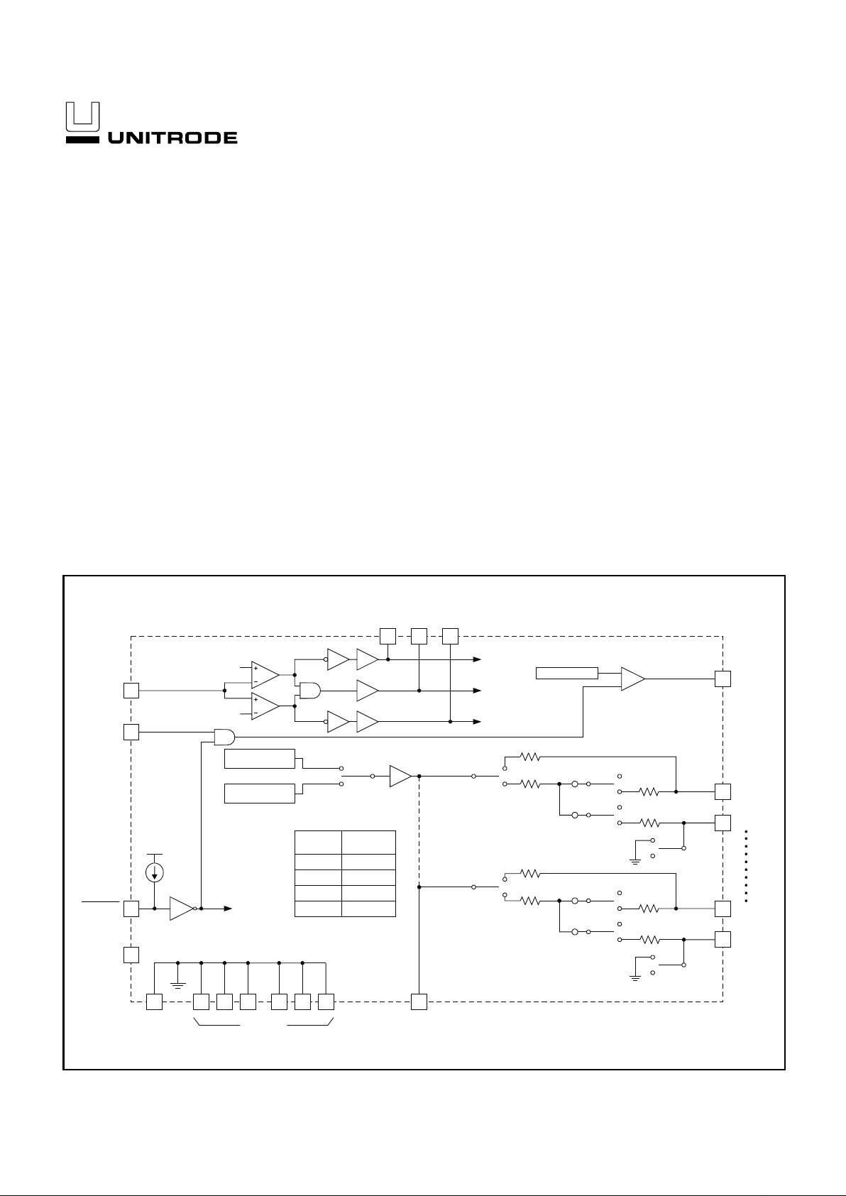
The UCC5631A Multimode SCSI Terminator provides a smooth transition
into the next generation of the SCSI Parallel Interface (SPI-2). It automati
-
cally senses the bus, via DIFFB, and switches the termination to either sin
gle ended (SE) or low voltage differential (LVD) SCSI, dependent on which
type of devices are connected to the bus.The UCC5631A can not be used
on a HVD, EIA485, differential SCSI bus. If the UCC5631A detects a HVD
SCSI device, it switches to a high impedance state.
The Multimode terminator contains all functions required to terminate and
auto detect and switch modes for SPI-2 bus architectures. Single Ended
and Differential impedances and currents are trimmed for maximum effec
tiveness. Fail Safe biasing is provided to insure signal integrity. Device/Bus
type detection circuitry is integrated into the terminator to provide automatic
switching of termination between single ended and LVD SCSI and a high
impedance for HVD SCSI. The multimode function provides all the perfor
mance analog functions necessary to implement SPI-2 termination in a sin
gle monolithic device.
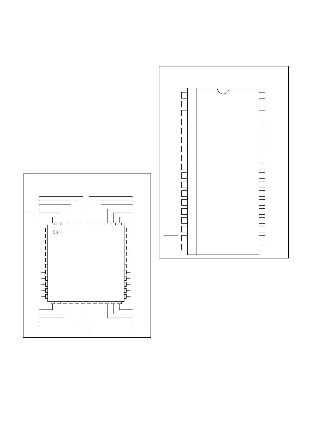
The UCC5631A is offered in a 36 pin SSOP package, as well as a 48 pin
LQFP package for a temperature range of 0°C to 70°C.
Multimode SCSI 9 Line Terminator
FEATURES
•
Auto Selection Single Ended (SE) or
Low Voltage Differential (LVD)
Termination
•
Meets SCSI-1, SCSI-2, SCSI-3, SPI,
Ultra (Fast-20), Ultra2 (SPI-2 LVD)
and Ultra3 Standards
•
2.7V to 5.25V Operation
•
Differential Failsafe Bias
•
Thermal packaging for low junction
temperature and better MTBF
•
Master/Slave Input
•
Supports Active Negation
•
3pF Channel Capacitance
• Reversed Disconnect Polarity
SLUS443 - OCTOBER 1999
LVDREF 1.25V
17
DISCNCT
REG
L1+
L9–
L9+
SOURCE/SINK REGULATOR
REF 1.3V
20 DIFSENS
–15mA ≤ I
SOURCE
≤ –5mA
50µA ≤ I
SINK
≤ 200µA
HIPD
LVD
SE
21DIFFB
0.6V
2.15V
52.5
32
52.5
31
110
1
SE REF 2.7V
SE GND SWITCH
36TRMPWR
18
GND
9
L1–
124
52.5
5
52.5
4
110
124
10µA
1.3V
(NOISE LOAD)
SE GND SWITCH
56mV
–+
+–
–+
56mV
56mV
56mV
+–
MODE
ALL
SWITCHES
SE
LVD
HIPD
DISCNCT
UP
DOWN
OPEN
OPEN
35
HIPD34LVD33SE
19
ENABLE
SWITCHES
MSTR/SLV
PATENTED CIRCUIT DESIGN
8
HS/GND
10 2726 28
BLOCK DIAGRAM
UDG-99165
Note: Indicated pinout is for 36 pin SSOP package.
2
UCC5631A
ABSOLUTE MAXIMUM RATINGS
TRMPWR Voltage . . . . . . . . . . . . . . . . . . . . . . . . . . . . . . . . . 6V
Signal Line Voltage . . . . . . . . . . . . . . . . . . . . . 0V to TRMPWR
Package Power Dissipation . . . . . . . . . . . . . . . . . . . . . . . . . 2W
Storage Temperature . . . . . . . . . . . . . . . . . . . –65°C to +150°C
Junction Temperature. . . . . . . . . . . . . . . . . . . –55°C to +150°C
Lead Temperature (Soldering, 10sec.) . . . . . . . . . . . . . +300°C
All voltages are with respect to pin 18. Currents are positive
into, negative out of the specified terminal. Consult Packaging
Section of the Databook for thermal limitations and consider
-
ations of packages.
RECOMMENDED OPERATING CONDITIONS
TRMPWR Voltage . . . . . . . . . . . . . . . . . . . . . . . . 2.7V to 5.25V
L3+
HS/GND
L9–
L9+
L8–
TRMPWR
N/C
N/C
HS/GND
L2–
HS/GND
L1+
L1–
L2+
REG
HS/GND
L3–
L8+
HS/GND
HS/GND
L4+
L4–
14
13
12
11
10
9
8
7
6
5
4
3
2
1
23
24
25
26
27
28
29
30
31
32
33
34
35
36
18
17
16
15
DIFF B
MSTR/SLV
DIFSENS
19
20
21
22L5+
L5–
DISCNCT
GND
L7–
L7+
L6–
L6+
HIPD
LVD
SE
CONNECTION DIAGRAM
48
47
46
45
1
44
43
424140
393837
2
3
4
5
6
7
8
9
10
11
12
13
14
15
161718 19 202122 23 24
36
35
34
33
32
31
30
29
28
27
26
25
NC
L3+
L3–
L4+
L4–
HS/GND
GND
DISCNCT
L5+
HS/GND
HS/GND
L1+
L1–
L2+
L2–
NC
HS/GND
REG
NC
NC
TERMPWR
NC
LVD
HIPD
L8+
L8–
L9+
L9–
HS/GND
N/C
DIFFB
DIFSENS
L6+
HS/GND
L7+
L6–
L7–
HS/GND
HS/GND
HS/GND
L5–
HS/GND
HS/GND
SE
HS/GNDHS/GND
HS/GND
MSTR/SLV
LQFP-48 (Top View)
FQP Package
QSOP-36 (Top View)
MWP Package
 Loading...