


UCC5639
Multimode SCSI 15 Line Terminator with Reverse Disconnect
FEATURES
∙Auto Selection Single Ended (SE) or Low Voltage Differential (LVD) Termination
∙Meets SCSI-1, SCSI-2, SCSI-3, SPI, Ultra (Fast-20), Ultra2 (SPI-2 LVD) and Ultra3 Standards
∙2.7V to 5.25V Operation
∙Differential Failsafe Bias
∙Thermal packaging for low junction temperature and better MTBF.
DESCRIPTION
The UCC5639 Multimode SCSI Terminator provides a smooth transition into the next generation of the SCSI Parallel Interface (SPI-2). It automatically senses the bus, via DIFFB, and switches the termination to either single ended (SE) or low voltage differential (LVD) SCSI, dependent on which type of devices are connected to the bus. The UCC5639 can not be used on a HVD, EIA485, differential SCSI bus. If the UCC5639 detects a HVD SCSI device, it switches to a high impedance state.
The Multimode terminator contains all functions required to terminate and auto detect and switch modes for SPI-2 bus architectures. Single Ended and Differential impedances and currents are trimmed for maximum effectiveness. Fail Safe biasing is provided to insure signal integrity. Device/Bus type detection circuitry is integrated into the terminator to provide automatic switching of termination between single ended and LVD SCSI and a high impedance for HVD SCSI. The multimode function provides all the performance analog functions necessary to implement SPI-2 termination in a single monolithic device.
The UCC5639 is offered in a 48 pin LQFP package for a temperature range of 0°C to 70°C.
BLOCK DIAGRAM
|
|
|
|
|
HIGH POWER |
|
(NOISE LOAD) |
|
|
|
2.05V |
|
|
|
|
|
|
|
|
|
|
|
|
DIFFERENTIAL |
|
REF |
1.3V |
|
|
|
|
|
|
|
LOW VOLTAGE |
|
1.3V |
35 |
DIFFSENS |
DIFFB |
34 |
|
|
|
|
|
|
|
|
|
|
|
DIFFERENTIAL |
|
|
|
|
||
|
|
|
|
|
|
–15mA ≤ ISOURCE ≤ –5mA |
|
||
|
0.6V |
|
|
|
|
|
|
||
|
|
|
|
SINGLE ENDED |
|
50μA ≤ ISINK |
≤ 200μA |
|
|
|
|
|
|
|
|
|
|||
|
|
REF |
|
|
|
110 |
|
|
|
|
|
SOURCE/SINK REGULATOR |
|
|
|
|
|||
|
|
2.7V |
|
|
|
|
|||
|
|
|
|
|
|
|
|
|
|
|
|
|
|
|
|
124 |
56mV |
52.5 |
|
|
|
|
|
|
|
|
|
||
|
|
|
|
|
|
|
|
|
|
|
|
REF |
|
|
|
|
– + |
12 |
L1– |
|
|
1.25V |
|
|
|
|
56mV |
|
|
|
|
|
|
|
|
|
52.5 |
|
|
|
|
|
|
|
|
|
|
|
|
|
|
|
MODE |
ALL SWITCHES |
|
+ – |
11 |
L1+ |
|
|
|
|
SE |
|
UP |
|
|
|
|
|
|
|
LVD |
|
DOWN |
|
SE GND SWITCH |
|
|
|
|
|
DISCNCT |
OPEN |
110 |
|
|
|
|
|
|
|
|
|
|
|
|
|
|
DISCNCT |
36 |
|
|
|
|
124 |
56mV |
52.5 |
|
|
|
|
|
|
|
||||
|
|
|
|
|
|
|
|
|
|
|
|
|
|
|
|
|
– + |
2 |
L15– |
|
|
|
|
|
|
|
56mV |
52.5 |
|
|
|
|
|
|
|
|
|
|
|
|
|
|
|
|
|
|
+ – |
1 |
L15+ |
TRMPWR |
3 |
|
|
|
|
|
SE GND SWITCH |
|
|
|
|
|
|
|
|
|
|
||
|
|
HS/GND |
HS/GND |
REG |
|
|
|
|
|
|
27 |
4-9 |
|
28-33 |
10 |
|
|
|
|
|
GND |
|
|
|
4.7μF . |
|
|
|
|
|
|
|
|
|
|
|
|
|
UDG-98110 |
03/99 |
|
|
|
|
|
|
|
|
|
UCC5639
ABSOLUTE MAXIMUM RATINGS
TRMPWR Voltage . . . . . . . . . . . . . . . . . . . . . . . . . . . . . . . . +6V Signal Line Voltage . . . . . . . . . . . . . . . . . . . . . 0V to TRMPWR Package Dissipation . . . . . . . . . . . . . . . . . . . . . . . . . . . . . . . 2W Storage Temperature . . . . . . . . . . . . . . . . . . . –65°C to +150°C Junction Temperature. . . . . . . . . . . . . . . . . . . –55°C to +150°C Lead Temperature (Soldering, 10 sec.) . . . . . . . . . . . . . +300°C Recommended Operating Conditions . . . . . . . . . 2.7V to 5.25V
Currents are positive into negative out of the specified terminal. Note: Consult Packaging Section of Databook for thermal limitations and considerations of package.
RECOMMENDED OPERATING CONDITIONS
TRMPWR Voltage . . . . . . . . . . . . . . . . . . . . . . . . 2.7V to 5.25V Temperature Ranges . . . . . . . . . . . . . . . . . . . . . . 0°C to +70°C
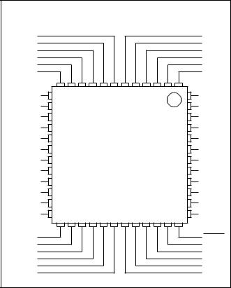
CONNECTION DIAGRAMS
(TOP VIEW) |
|
|
|
|
|
|
|
|
|
|
|
|
|
FQP Package |
|
|
|
|
|
|
|
|
|
|
|
|
|
HS/GND |
|
|
|
|
|
|
|
|
|
|
|
|
HS/GND |
HS/GND |
|
|
|
|
|
|
|
|
|
|
|
|
HS/GND |
HS/GND |
|
|
|
|
|
|
|
|
|
|
|
|
HS/GND |
REG |
|
|
|
|
|
|
|
|
|
|
|
|
TRMPWR |
L1+ |
|
|
|
|
|
|
|
|
|
|
|
|
L15– |
L1– |
|
|
|
|
|
|
|
|
|
|
|
|
L15+ |
L2+ |
12 |
11 |
10 |
9 |
8 |
7 |
6 |
5 |
4 |
3 |
2 |
1 |
L14– |
13 |
|
|
|
|
|
|
|
|
|
|
48 |
||
L2– |
14 |
|
|
|
|
|
|
|
|
|
|
47 |
L14+ |
L3+ |
15 |
|
|
|
|
|
|
|
|
|
|
46 |
L13– |
L3– |
16 |
|
|
|
|
|
|
|
|
|
|
45 |
L13+ |
L4+ |
17 |
|
|
|
|
|
|
|
|
|
|
44 |
L12– |
|
|
|
|
|
|
|
|
|
|
|
|||
L4– |
18 |
|
|
|
|
|
|
|
|
|
|
43 |
L12+ |
|
|
|
|
|
|
|
|
|
|
|
|||
L5+ |
19 |
|
|
|
|
|
|
|
|
|
|
42 |
L11– |
|
|
|
|
|
|
|
|
|
|
|
|||
L5– |
20 |
|
|
|
|
|
|
|
|
|
|
41 |
L11+ |
|
|
|
|
|
|
|
|
|
|
|
|||
L6+ |
21 |
|
|
|
|
|
|
|
|
|
|
40 |
L10– |
L6– |
22 |
|
|
|
|
|
|
|
|
|
|
39 |
L10+ |
L7+ |
23 |
|
|
|
|
|
|
|
|
|
|
38 |
L9– |
L7– |
24 |
|
|
|
|
|
|
|
|
|
|
37 |
L9+ |
|
25 |
26 |
27 |
28 |
29 |
30 |
31 |
32 |
33 |
34 |
35 |
36 |
|
L8+ |
|
|
|
|
|
|
|
|
|
|
|
|
DISCNCT |
L8– |
|
|
|
|
|
|
|
|
|
|
|
|
DIFSENS |
GND |
|
|
|
|
|
|
|
|
|
|
|
|
DIFFB |
HS/GND |
|
|
|
|
|
|
|
|
|
|
|
|
HS/GND |
HS/GND |
|
|
|
|
|
|
|
|
|
|
|
|
HS/GND |
HS/GND |
|
|
|
|
|
|
|
|
|
|
|
|
HS/GND |
ELECTRICAL CHARACTERISTICS Unless otherwise stated, these specifications apply for TA = TJ = 0°C to 70°C, TRMPWR = 3.3V.
|
PARAMETER |
TEST CONDITIONS |
MIN |
TYP |
MAX |
UNITS |
TRMPWR Supply Current Section |
|
|
|
|
|
|
TRMPWR Supply Current |
LVD Mode |
|
20 |
25 |
mA |
|
|
|
SE Mode |
|
1.6 |
10 |
mA |
|
|
Disabled Terminator |
|
250 |
400 |
μA |
Regulator Section |
|
|
|
|
|
|
1.25V Regulator |
LVD Mode |
1.15 |
1.25 |
1.35 |
V |
|
1.25V Regulator Source Current |
VREG= 0V |
–375 |
–700 |
–1000 |
mA |
|
1.25V Regulator Sink Current |
VREG= 3.3V |
170 |
300 |
700 |
mA |
|
1.3V |
Regulator |
DIFSENS |
1.2 |
1.3 |
1.4 |
V |
1.3V |
Regulator Source Current |
VREG= 0V |
–15 |
|
–5 |
mA |
1.3V |
Regulator Sink Current |
VREG= 3.3V |
50 |
|
200 |
μA |
2.7V |
Regulator |
SE Mode |
2.5 |
2.7 |
3.0 |
V |
2.7V |
Regulator Source Current |
VREG= 0V |
–375 |
–700 |
–1000 |
mA |
2.7V |
Regulator Sink Curren |
VREG= 3.3V |
170 |
300 |
700 |
mA |
Differential Termination Section |
|
|
|
|
|
|
Differential Impedance |
|
100 |
105 |
110 |
Ω |
|
Common Mode Impedence |
(Note 2) |
110 |
150 |
165 |
Ω |
|
Differential Bias Voltage |
|
100 |
|
125 |
mV |
|
Common Mode Bias |
|
1.15 |
1.25 |
1.35 |
V |
|
Output Capacitance |
Single Ended Measurement to Ground (Note 1) |
|
|
3 |
pF |
|
2
 Loading...