Motorola MCR310-8, MCR310-2, MCR310-3, MCR310-4, MCR310-6 Datasheet
...
MOTOROLA
SEMICONDUCTOR TECHNICAL DATA
Order this document by MCR310/D
Silicon Controlled Rectifiers
Reverse Blocking Triode Thyristors
. . . designed for industrial and consumer applications such as temperature, light and speed control; process and remote controls; warning systems; capacitive discharge circuits and MPU interface.
•Center Gate Geometry for Uniform Current Density
•All Diffused and Glass-Passivated Junctions for Parameter Uniformity and Stability
•Small, Rugged, Thermowatt Construction for Low Thermal Resistance, High Heat Dissipation and Durability
•Low Trigger Currents, 200 μA Maximum for Direct Driving from Integrated Circuits
MAXIMUM RATINGS (TJ = 25°C unless otherwise noted.)
Rating |
Symbol |
Value |
Unit |
|
|
|
|
Peak Repetitive Forward and Reverse Blocking |
VDRM |
|
Volts |
Voltage(1) |
or |
|
|
(TJ = ±40 to 110°C) |
VRRM |
|
|
(1/2 Sine Wave, RGK = 1 kΩ) |
|
50 |
|
MCR310-2 |
|
|
|
MCR310-3 |
|
100 |
|
MCR310-4 |
|
200 |
|
MCR310-6 |
|
400 |
|
MCR310-8 |
|
600 |
|
MCR310-10 |
|
800 |
|
|
|
|
|
On-State RMS Current (TC = 75°C) |
IT(RMS) |
10 |
Amps |
Peak Non-repetitive Surge Current |
ITSM |
100 |
Amps |
(1/2 Cycle, 60 Hz, TJ = ±40 to 110°C) |
|
|
|
Circuit Fusing (t = 8.3 ms) |
I2t |
40 |
A2s |
Peak Gate Voltage (t p 10 μs) |
VGM |
±5 |
Volts |
Peak Gate Current (t p 10 μs) |
IGM |
1 |
Amp |
Peak Gate Power (t p 10 μs) |
PGM |
5 |
Watts |
Average Gate Power |
PG(AV) |
0.75 |
Watt |
Operating Junction Temperature Range |
TJ |
±40 to +110 |
°C |
Storage Temperature Range |
Tstg |
±40 to +150 |
°C |
Mounting Torque |
± |
8 |
in.-lb. |
|
|
|
|
THERMAL CHARACTERISTICS |
|
|
|
Characteristic |
Symbol |
Max |
Unit |
|
|
|
|
Thermal Resistance, Junction to Case |
RθJC |
2.2 |
°C/W |
Thermal Resistance, Junction to Ambient |
RθJA |
60 |
°C/W |
MCR310
Series
SCRs
10 AMPERES RMS
50 thru 800 VOLTS
 G A
G A 
 C
C
K
A |
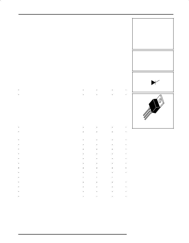
CASE 221A-04 |
G |
(TO-220AB) |
|
STYLE 3 |
1.VDRM and VRRM for all types can be applied on a continuous basis. Ratings apply for zero or negative gate voltage; however, positive gate voltage shall not be applied concurrent with negative potential on the anode. Blocking voltages shall not be tested with a constant current source such that the voltage ratings of the devices are exceeded.
Motorola, Inc. 1995

MCR310 Series
ELECTRICAL CHARACTERISTICS (TC = 25°C, RGK = 1 kΩ unless otherwise noted)
Characteristic |
|
Symbol |
Min |
Typ |
Max |
Unit |
|
|
|
|
|
|
|
Peak Forward Blocking Current(1) |
T = 110°C |
I |
Ð |
Ð |
500 |
μA |
|
C |
DRM |
|
|
|
|
(TJ = 110°C, VD = Rated VDRM) |
TC = 25°C |
|
Ð |
Ð |
10 |
μA |
Peak Reverse Blocking Current(1) |
T = 110°C |
I |
Ð |
Ð |
500 |
μA |
|
C |
RRM |
|
|
|
|
(TJ = 110°C, VR = Rated VRRM) |
TC = 25°C |
|
Ð |
Ð |
10 |
μA |
On-State Voltage |
|
VTM |
Ð |
1.7 |
2.2 |
Volts |
(ITM = 20 A Peak, Pulse Width p 1 ms, Duty Cycle p 2%) |
|
|
|
|
|
|
Gate Trigger Current, Continuous dc(2) |
|
I |
Ð |
30 |
200 |
μA |
(VD = 12 V, RL = 100 Ω) |
|
GT |
|
|
|
|
|
|
|
|
|
|
|
Gate Trigger Voltage, Continuous dc |
|
VGT |
|
|
|
Volts |
(VD = 12 V, RL = 100 Ω) |
|
|
Ð |
0.5 |
1.5 |
|
(VD = Rated VDRM, RL = 10 kΩ, TJ = 110°C) |
|
|
0.1 |
Ð |
Ð |
|
Holding Current |
|
IH |
Ð |
Ð |
6 |
mA |
(VD = 12 V, ITM = 100 mA) |
|
|
|
|
|
|
Critical Rate of Rise of Forward Blocking Voltage |
dv/dt |
Ð |
10 |
Ð |
V/μs |
|
(VD = Rated VDRM, TJ = 110°C, Exponential Waveform) |
|
|
|
|
|
|
Gate Controlled Turn-On Time |
|
tgt |
Ð |
1 |
Ð |
μs |
(VD = Rated VDRM, ITM = 20 A, IG = 2 mA) |
|
|
|
|
|
|
1.Ratings apply for negative gate voltage or RGK = 1 kΩ. Devices shall not have a positive gate voltage concurrently with a negative voltage on the anode. Devices should not be tested with a constant current source for forward and reverse blocking capability such that the voltage applied exceeds the rated blocking voltage.
2.Does not include RGK current.
°C) |
120 |
|
|
|
|
|
|
|
|
|
|
|
|
( |
|
|
|
|
|
|
TEMPERATURE |
110 |
|
|
|
α |
|
|
|
|
|
|
||
|
|
|
α = CONDUCTION ANGLE |
|
||
100 |
|
|
|
|
|
|
|
|
|
|
|
|
|
CASE |
90 |
α = 30° |
|
|
|
|
|
60° 90° |
|
|
|
||
, MAXIMUM |
|
|
|
|
||
|
|
180° |
|
|
||
80 |
|
|
|
|
||
|
|
|
|
|
||
|
|
|
|
|
|
|
C |
|
|
|
|
dc |
|
T |
70 |
|
|
|
|
|
|
|
|
|
|
|
|
|
0 |
2 |
4 |
6 |
8 |
10 |
|
|
IT(AV), AVERAGE ON-STATE CURRENT (AMPS) |
|
|||
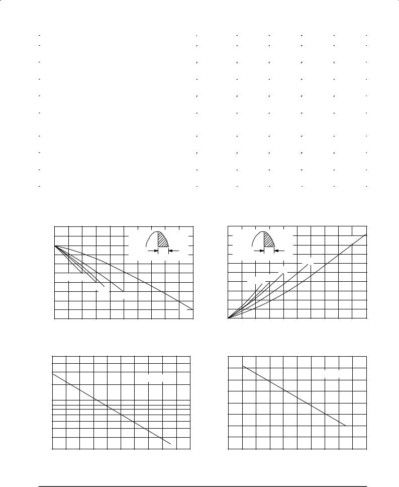
Figure 1. Average Current Derating
(WATTS) |
20 |
|
|
|
|
|
|
|
|
|
|
dc |
|
DISSIPATION |
16 |
|
|
|
|
|
α |
|
|
|
|
||
|
|
|
|
|
||
|
α = CONDUCTION ANGLE |
180° |
|
|
||
12 |
|
|
|
|
||
|
90° |
|
|
|
||
|
|
|
|
|
||
POWER |
|
|
|
|
|
|
8 |
α = 30° 60° |
|
|
|
|
|
, AVERAGE |
4 |
|
|
|
|
|
|
|
|
|
|
|
|
AV |
|
|
|
|
|
|
P |
0 |
|
|
|
|
|
|
|
|
|
|
|
|
|
0 |
2 |
4 |
6 |
8 |
10 |
|
|
IT(AV), AVERAGE ON-STATE CURRENT (AMPS) |
|
|||
Figure 2. On-State Power Dissipation
NORMALIZED GATE CURRENT
3
2
VD = 12 Vdc
1
0.5
0.3
±40 |
±20 |
0 |
20 |
40 |
60 |
80 |
90 |
100 |
120 |
140 |
|
|
|
TJ, JUNCTION TEMPERATURE (°C) |
|
|
|
||||
Figure 3. Normalized Gate Current
VGT, GATE TRIGGER VOLTAGE (VOLTS)
0.7
VD = 12 Vdc
0.6
0.5
0.4
0.3
0.2
0.1
±60 |
±40 |
±20 |
0 |
20 |
40 |
60 |
80 |
100 |
120 |
|
|
|
TJ, JUNCTION TEMPERATURE (°C) |
|
|
||||
Figure 4. Gate Voltage
2 |
Motorola Thyristor Device Data |
 Loading...