Motorola MCR102, MCR103 Datasheet

MOTOROLA
SEMICONDUCTOR TECHNICAL DATA
Order this document by MCR102/D
Silicon Controlled Rectifiers
Reverse Blocking Triode Thyristors
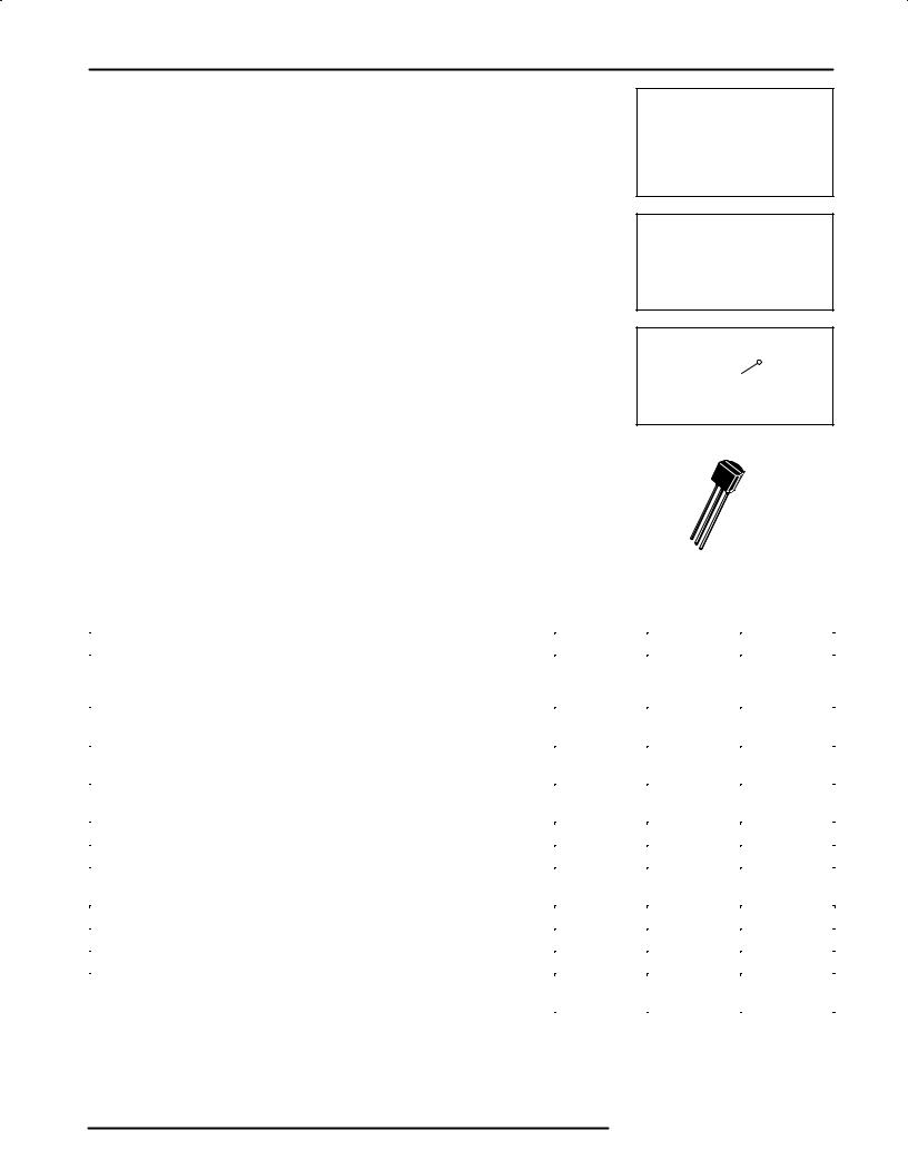
Annular PNPN devices designed for low cost, high volume consumer applications such as relay and lamp drivers, small motor controls, gate drivers for larger thyristors, and sensing and detection circuits. Supplied in an inexpensive plastic TO-226AA package which is readily adaptable for use in automatic insertion equipment.
•Sensitive Gate Trigger Current Ð 200 μA Maximum
•Low Reverse and Forward Blocking Current Ð 100 μA Maximum, TC = 85°C
•Low Holding Current Ð 5 mA Maximum
•Passivated Surface for Reliability and Uniformity
MCR102
MCR103
SCRs
0.8 AMPERES RMS
30 and 60 VOLTS
G
A

 K
K
|
|
|
|
K G |
|
|
|
|
|
|
A CASE 29-04 |
||
|
|
|
|
(TO-226AA) |
||
|
|
|
|
|
STYLE 10 |
|
MAXIMUM RATINGS (TJ = 25°C unless otherwise noted.) |
|
|
|
|
|
|
|
|
|
|
|
||
|
|
|
|
|
|
|
Rating |
|
Symbol |
Value |
|
Unit |
|
|
|
|
|
|
|
|
Peak Repetitive Forward and Reverse Blocking Voltage(2) |
VDRM |
|
|
Volts |
||
(TC = + 85°C, RGK = 1 kΩ) |
MCR102 |
VRRM |
30 |
|
|
|
|
MCR103 |
|
|
60 |
|
|
|
|
|
|
|
|
|
Forward Current RMS (See Figures 1 & 2) |
|
IT(RMS) |
0.8 |
|
Amps |
|
(All Conduction Angles) |
|
|
|
|
|
|
|
|
|
|
|
|
|
Peak Forward Surge Current, TA = 25°C |
|
ITSM |
10 |
|
Amps |
|
(1/2 Cycle, Sine Wave, 60 Hz) |
|
|
|
|
|
|
|
|
|
|
|
|
|
Circuit Fusing Considerations |
|
I2t |
0.415 |
|
A2s |
|
(t = 8.3 ms) |
|
|
|
|
|
|
|
|
|
|
|
|
|
Peak Gate Power Ð Forward, T A = 25°C |
|
PGM |
0.1 |
|
Watt |
|
Average Gate Power Ð Forward, T A = 25°C |
|
PGF(AV) |
0.01 |
|
Watt |
|
Peak Gate Current Ð Forward, T A = 25°C |
|
IGFM |
1 |
|
Amp |
|
(300 μs, 120 PPS) |
|
|
|
|
|
|
|
|
|
|
|
|
|
Peak Gate Voltage Ð Reverse |
|
VGRM |
4 |
|
Volts |
|
Operating Junction Temperature Range @ Rated VRRM and VDRM |
TJ |
±40 to +85 |
|
°C |
||
Storage Temperature Range |
|
Tstg |
±40 to +150 |
|
°C |
|
Lead Solder Temperature |
|
Ð |
|
+ 230 |
|
°C |
(t 1/16I from case, 10 s max) |
|
|
|
|
|
|
|
|
|
|
|
|
|
1.Temperature reference point for all case temperature is center of flat portion of package. (TC = +85°C unless otherwise noted.)
2.VDRM and VRRM for all types can be applied on a continuous dc basis without incurring damage. Ratings apply for zero or negative gate voltage but positive gate voltage shall not be applied concurrently with a negative potential on the anode. When checking forward or reverse blocking capability, thyristor devices should not be tested with a constant current source in a manner that the voltage applied exceeds the rated blocking voltage.
Motorola, Inc. 1995

MCR102 MCR103
THERMAL CHARACTERISTICS
Characteristic |
|
|
|
Symbol |
|
Max |
|
|
Unit |
|
|
|
|
|
|
|
|
|
|
|
|
Thermal Resistance, Junction to Case |
|
|
|
RθJC |
75 |
|
|
°C/W |
||
Thermal Resistance, Junction to Ambient |
|
|
|
RθJA |
200 |
|
|
°C/W |
||
ELECTRICAL CHARACTERISTICS (TC = 25°C, RGK = 1000 Ω unless otherwise specified.) |
|
|
|
|
|
|
||||
Characteristic |
|
|
|
Symbol |
|
Min |
Max |
|
Unit |
|
|
|
|
|
|
|
|
|
|
|
|
Peak Forward or Reverse Blocking Current |
|
TC = 25°C |
IDRM, IRRM |
|
Ð |
10 |
|
μA |
||
(VAK = Rated VDRM or VRRM) |
|
|
|
|
||||||
|
|
TC = 85°C |
|
|
Ð |
100 |
|
μA |
||
(1) |
|
|
|
VTM |
|
Ð |
1.7 |
|
Volts |
|
Forward ªOnº Voltage |
|
|
|
|
|
|||||
(ITM = 1 A Peak @ TA = 25°C) |
|
|
|
|
|
|
|
|
|
|
Gate Trigger Current (Continuous dc)(2) |
T |
C |
= 25°C |
I |
|
Ð |
200 |
|
μA |
|
(Anode Voltage = 7 Vdc, RL = 100 Ohms) |
|
|
GT |
|
|
|
|
|
|
|
|
|
|
|
|
|
|
|
|
|
|
Gate Trigger Voltage (Continuous dc) |
|
TC = 25°C |
VGT |
|
Ð |
0.8 |
|
Volts |
||
(Anode Voltage = 7 Vdc, RL = 100 Ohms) |
|
TC = ±65°C |
VGD |
|
Ð |
1.2 |
|
|
||
|
|
TC = 85°C |
|
|
0.1 |
Ð |
|
|
||
Holding Current |
TC = 25°C |
IH |
|
Ð |
5 |
|
mA |
|||
(Anode Voltage = 7 Vdc, initiating current = 20 mA) |
TC = ±65°C |
|
|
Ð |
10 |
|
|
|||
1.Forward current applied for 1 ms maximum duration, duty cycle p 1%.
2.RGK current is not included in measurement.
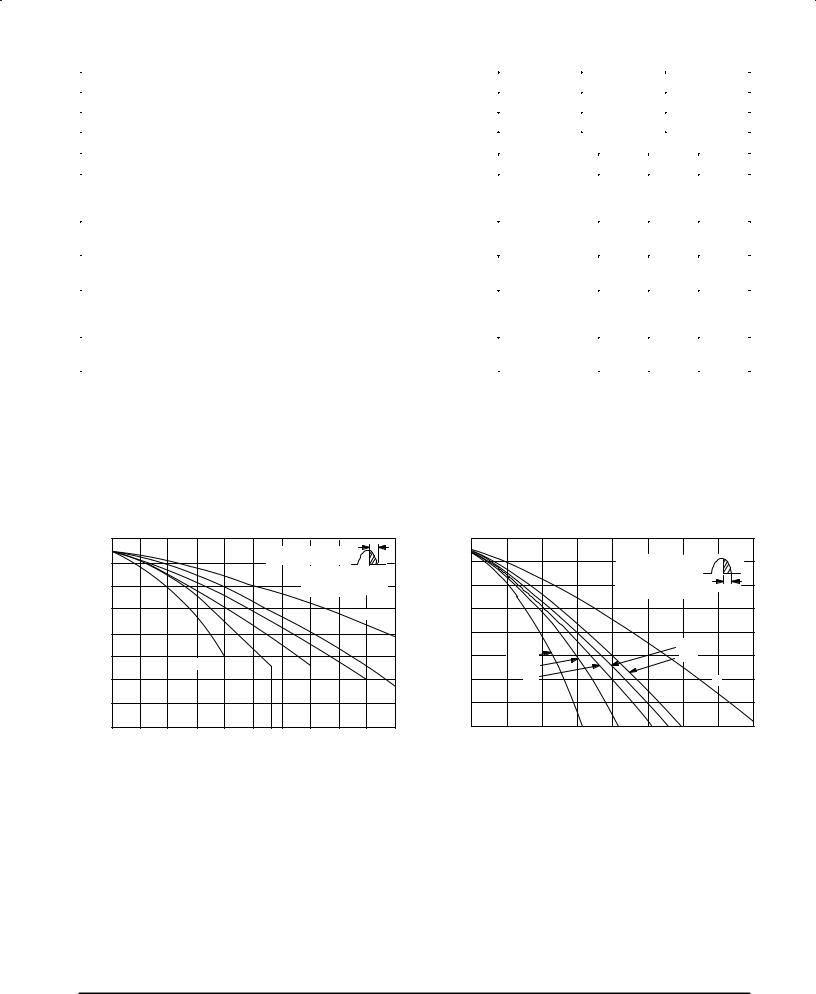
FIGURE 1 ± CURRENT DERATING (REFERENCE: CASE TEMPERATURE)
FIGURE 2 ± CURRENT DERATING (REFERENCE: AMBIENT TEMPERATURE)
CASE TEMPERATURE (°C)
TC , MAXIMUM ALLOWABLE
90 |
|
|
|
α = CONDUCTION |
α |
|
|
90 |
|
|
|
|
|
|
|
|
|
|
|
|
|
|
|
|
|
||
|
|
|
|
|
ANGLE |
|
|
(TEMPERATURE°C) |
|
|
α = CONDUCTION ANGLE |
|
|
|
|
|
|
|
CASE MEASUREMENT |
ALLOWABLEMAXIMUM, |
|
|
TYPICAL PRINTED |
α |
|||
|
|
|
60° |
|
90° |
|
|
60 |
|
|
|||
|
|
|
|
|
|
|
|
|
|||||
70 |
|
|
|
|
POINT ± CENTER OF |
|
|
70 |
|
CIRCUIT BOARD |
|
|
|
|
|
|
|
FLAT PORTION |
|
|
|
|
|
|
|||
|
|
|
|
|
|
|
|
|
|
MOUNTING |
|
|
|
|
|
|
|
|
dc |
|
|
|
|
|
|
|
|
50 |
|
|
|
|
|
|
|
|
50 |
|
|
120° |
|
|
|
|
|
|
|
|
|
|
|
α = 30° |
|
|
|
|
|
α = 30° |
|
|
120° |
180° |
T AMBIENT |
|
|
180° |
|
||
|
|
|
|
|
° |
|
|
|
|||||
30 |
|
|
|
|
|
|
A |
|
30 |
90° |
|
|
dc |
10 |
|
|
|
|
|
|
|
|
10 |
|
|
|
|
0 |
0.1 |
0.2 |
|
0.3 |
0.4 |
0.5 |
|
|
0 |
0.1 |
0.2 |
0.3 |
0.4 |
|
I |
, AVERAGE FORWARD CURRENT (AMP) |
|
|
|
|
IF(AV), AVERAGE FORWARD CURRENT (AMP) |
|
|||||
|
F(AV) |
|
|
|
|
|
|
|
|
|
|
|
|
2 |
Motorola Thyristor Device Data |
 Loading...