


Motorola MCM6946YJ12R, MCM6946YJ15, MCM6946YJ15R, MCM6946YJ8, MCM6946YJ8R Datasheet
...MOTOROLA
SEMICONDUCTOR TECHNICAL DATA
Order this document by MCM6946/D
Advance Information
512K x 8 Bit Static Random
Access Memory
The MCM6946 is a 4,194,304±bit static random access memory organized as 524,288 words of 8 bits. Static design eliminates the need for external clocks or timing strobes.
The MCM6946 is equipped with chip enable (E) and output enable (G) pins, allowing for greater system flexibility and eliminating bus contention problems. Either input, when high, will force the outputs into high±impedance.
The MCM6946 is available in a 400 mil, 36±lead surface±mount SOJ package.
•Single 3.3 V ± 5%, + 10% Power Supply
•Fast Access Time: 8/10/12/15 ns
•Equal Address and Chip Enable Access Time
•All Inputs and Outputs are TTL Compatible
•Three±State Outputs
•Power Operation: 195/185/180/175 mA Maximum, Active AC
•Available in TSOP or SOJ Packages
MCM6946
YJ PACKAGE 400 MIL SOJ CASE 893±02
TS PACKAGE 44±LEAD TSOP TYPE II CASE 924A±02
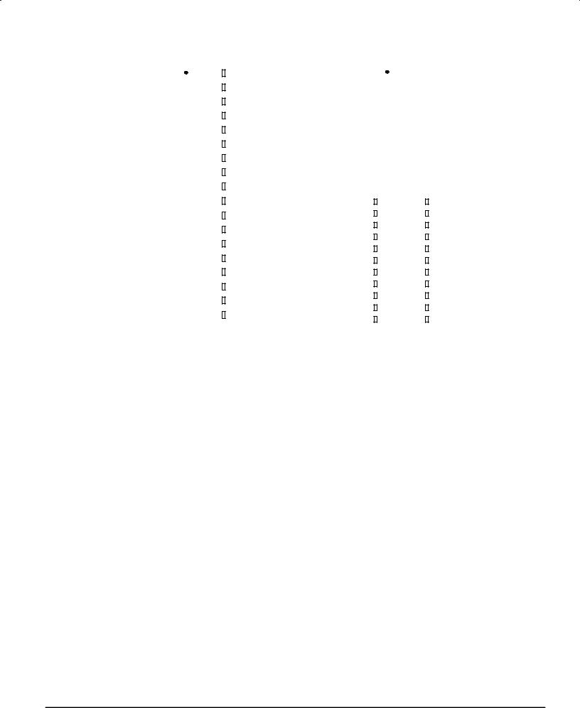
PIN NAMES
A0 ± A18 . . . . . . . . . . . . . . . Address Inputs
W . . . . . . . . . . . . . . . . . . . . . . . Write Enable
G . . . . . . . . . . . . . . . . . . . . . Output Enable
E . . . . . . . . . . . . . . . . . . . . . . . . Chip Enable
DQ . . . . . . . . . . . . . . . . . Data Input/Output
NC . . . . . . . . . . . . . . . . . . . . No Connection
VCC . . . . . . . . . . . . . + 3.3 V Power Supply
VSS . . . . . . . . . . . . . . . . . . . . . . . . . Ground
This document contains information on a new product. Specifications and information herein are subject to change without notice.
REV 5 3/31/98
Motorola, Inc. 1998 |
MCM6946 |
MOTOROLA FAST SRAM |
|
|
1 |

BLOCK DIAGRAM
A |
|
|
|
A |
|
|
|
A |
|
|
|
A |
|
|
|
A |
ROW |
|
|
|
MEMORY MATRIX |
||
A |
DECODER |
||
|
|||
A |
|
|
|
A |
|
|
|
A |
|
|
|
A |
|
|
DQ |
|
|
COLUMN I/O |
|
|
|
||
INPUT |
|
|
COLUMN DECODER |
|
|
|
||
DATA |
|
|
|
|
|
|
|
|
CONTROL |
|
|
|
|
|
|
|
|
DQ |
|
|
|
|
|
|
|
|
A |
A |
A |
A |
A |
A |
A |
A |
A |
|
|
|
|
|
|
|
|
DQ |
E |
|
|
|
|
|
|
|
|
W |
DQ |
|
G |
||
|
MCM6946 |
MOTOROLA FAST SRAM |
2 |
|
|
|
|
|
|
|
|
|
|
|
|
PIN ASSIGNMENTS |
|
|
|
|
|
|
|
||||
|
|
|
|
|
400 MIL SOJ |
|
|
|
|
|
|
|
|
TSOP TYPE II |
|
|
|
|||||
|
|
|
|
|
|
|
|
|
|
|
NC |
|
|
|
|
|
|
|
||||
|
|
A |
|
1 |
36 |
NC |
|
1 |
44 |
|
|
NC |
||||||||||
|
|
|
|
|
||||||||||||||||||
|
|
A |
|
2 |
35 |
A |
NC |
|
2 |
43 |
|
|
NC |
|||||||||
|
|
|
|
|
||||||||||||||||||
|
|
|
|
|
A |
|
3 |
42 |
|
|
NC |
|||||||||||
|
|
A |
|
3 |
34 |
|
A |
|
|
|
|
|
||||||||||
|
|
|
|
|
|
|||||||||||||||||
|
|
|
|
|
|
A |
|
4 |
41 |
|
|
A |
||||||||||
|
|
A |
|
4 |
33 |
|
A |
|
|
|
|
|
||||||||||
|
|
|
|
|
|
A |
|
5 |
40 |
|
|
A |
||||||||||
|
A |
|
5 |
32 |
|
A |
|
|
|
|
|
|||||||||||
|
|
|
|
|
A |
|
6 |
39 |
|
|
A |
|||||||||||
|
|
|
|
|
|
|
|
|||||||||||||||
|
|
|
|
|
|
6 |
31 |
|
|
|
|
|
A |
|
7 |
38 |
|
|
A |
|||
|
|
E |
|
|
|
|
G |
|
|
|
||||||||||||
|
|
|
|
|
|
|
|
|
||||||||||||||
|
|
|
|
|
|
|
|
|
|
|
|
|
|
|
|
|
8 |
37 |
|
|
|
|
DQ |
|
7 |
30 |
DQ |
E |
|
|
G |
||||||||||||||
|
DQ |
|
9 |
36 |
|
|
DQ |
|||||||||||||||
DQ |
|
8 |
29 |
DQ |
|
|
|
|||||||||||||||
|
DQ |
|
10 |
35 |
|
|
DQ |
|||||||||||||||
VCC |
|
9 |
28 |
|
VSS |
|
|
|
||||||||||||||
|
|
VDD |
|
11 |
34 |
|
|
VSS |
||||||||||||||
|
|
|
|
|||||||||||||||||||
|
||||||||||||||||||||||
|
|
|
|
|
|
|||||||||||||||||
VSS |
|
10 |
27 |
|
VCC |
VSS |
|
12 |
33 |
|
|
VDD |
||||||||||
|
||||||||||||||||||||||
DQ |
|
11 |
26 |
|
DQ |
DQ |
|
13 |
32 |
|
|
DQ |
||||||||||
|
||||||||||||||||||||||
DQ |
|
12 |
25 |
|
DQ |
DQ |
|
14 |
31 |
|
|
DQ |
||||||||||
|
|
|||||||||||||||||||||
|
|
|
|
|
|
|
|
15 |
30 |
|
|
A |
||||||||||
|
|
|
|
|
|
13 |
24 |
|
A |
|
W |
|
|
|
|
|||||||
|
W |
|
|
|
|
|
A |
|
16 |
29 |
|
|
A |
|||||||||
|
A |
|
14 |
23 |
|
A |
|
|
|
|
|
|||||||||||
|
|
|
|
|
A |
|
17 |
28 |
|
|
A |
|||||||||||
|
|
|
|
|
|
|
|
|
|
|
|
|
|
|
|
|||||||
|
A |
|
15 |
22 |
|
A |
|
|
A |
|
18 |
27 |
|
|
A |
|||||||
|
||||||||||||||||||||||
|
A |
|
16 |
21 |
|
A |
|
A |
|
19 |
26 |
|
|
A |
||||||||
|
|
|
||||||||||||||||||||
|
A |
|
17 |
20 |
|
A |
|
|
A |
|
20 |
25 |
|
|
NC |
|||||||
|
|
|
||||||||||||||||||||
|
|
|
NC |
|
21 |
24 |
|
|
NC |
|||||||||||||
|
|
A |
|
18 |
19 |
|
NC |
|
|
|
||||||||||||
|
|
|
|
NC |
|
22 |
23 |
|
|
NC |
||||||||||||
|
|
|
|
|
|
|
|
|
|
|
|
|
|
|||||||||
|
|
|
|
|
|
|
|
|
|
|
|
|
|
|
|
|
|
|
|
|
|
|
MOTOROLA FAST SRAM |
MCM6946 |
|
3 |

TRUTH TABLE (X = Don't Care)
|
|
|
|
|
|
|
|
|
|
|
|
|
|
E |
|
G |
|
W |
Mode |
I/O Pin |
Cycle |
Current |
|||
|
|
|
|
|
|
|
|
|
|
|||
H |
|
X |
|
|
X |
Not Selected |
High±Z |
Ð |
ISB1, ISB2 |
|||
|
L |
|
H |
|
|
H |
Output Disabled |
High±Z |
Ð |
ICCA |
||
|
L |
|
L |
|
|
H |
Read |
Dout |
Read |
ICCA |
||
|
L |
|
X |
|
|
L |
Write |
High±Z |
Write |
ICCA |
||
ABSOLUTE MAXIMUM RATINGS (See Note)
Rating |
Symbol |
Value |
|
Unit |
|
|
|
|
|
Power Supply Voltage Relative to VSS |
VCC |
± 0.5 to + |
5.0 |
V |
Voltage Relative to VSS for Any Pin |
Vin, Vout |
± 0.5 to VCC + 0.5 |
V |
|
Except VCC |
|
|
|
|
Output Current (per I/O) |
Iout |
± 20 |
|
mA |
Power Dissipation |
PD |
1.0 |
|
W |
Temperature Under Bias |
Tbias |
± 10 to + |
85 |
°C |
Operating Temperature |
TA |
0 to + 70 |
°C |
|
Storage Temperature Ð Plastic |
Tstg |
± 55 to + 150 |
°C |
|
NOTE: Permanent device damage may occur if ABSOLUTE MAXIMUM RATINGS are exceeded. Functional operation should be restricted to RECOMMENDED OPER-
ATING CONDITIONS. Exposure to higher than recommended voltages for extended periods of time could affect device reliability.
This device contains circuitry to protect the inputs against damage due to high static voltages or electric fields; however, it is advised that normal precautions be taken to avoid application of any voltage higher than maximum rated voltages to these high±impedance circuits.
This BiCMOS memory circuit has been designed to meet the dc and ac specifications shown in the tables, after thermal equilibrium has been established. The circuit is in a test socket or mounted on a printed circuit board and transverse air flow of at least 500 linear feet per minute is maintained.
MCM6946 |
MOTOROLA FAST SRAM |
4 |
|
 Loading...