Motorola MCR218-8FP, MCR218-2FP, MCR218-10FP, MCR218-6FP, MCR218-4FP Datasheet

MOTOROLA
SEMICONDUCTOR TECHNICAL DATA
Order this document by MCR218FP/D
MCR218FP
Series
Silicon Controlled Rectifiers
Reverse Blocking Thyristors
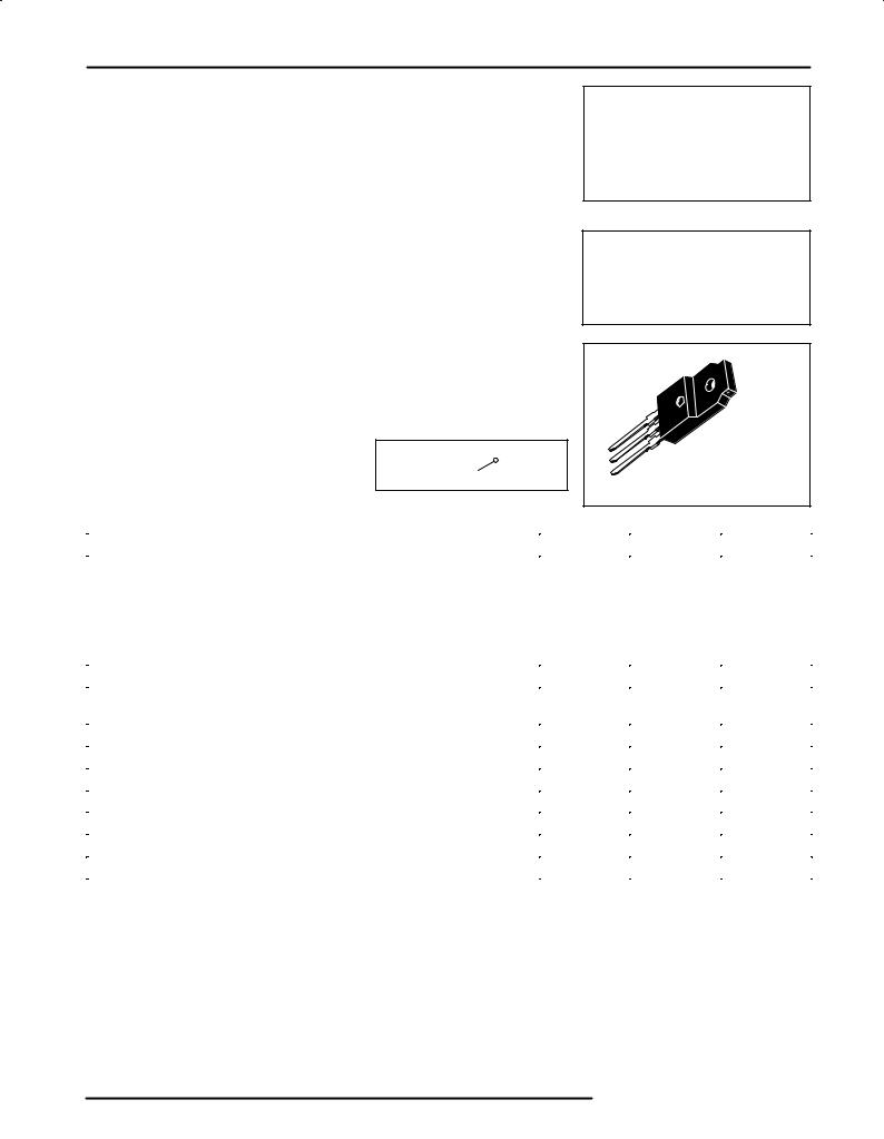
. . . designed primarily for half-wave ac control applications, such as motor controls, heating controls and power supply crowbar circuits.
•Glass Passivated Junctions with Center Gate Fire for Greater Parameter Uniformity and Stability
•Small, Rugged, Thermowatt Constructed for Low Thermal Resistance, High Heat Dissipation and Durability
•Blocking Voltage to 800 Volts
•80 A Surge Current Capability
•Insulated Package Simplifies Mounting
G
A 

 K
K
MAXIMUM RATINGS (TJ = 25°C unless otherwise noted.)
ISOLATED SCRs 8 AMPERES RMS 50 thru 800 VOLTS
CASE 221C-02
STYLE 2
Rating |
Symbol |
Value |
Unit |
|
|
|
|
|
|
Peak Repetitive Forward and Reverse Blocking Voltage(1) |
|
VDRM |
|
Volts |
(TJ = ±40 to +125°C, Gate Open) |
|
VRRM |
|
|
MCR218-2FP |
|
|
50 |
|
MCR218-4FP |
|
|
200 |
|
MCR218-6FP |
|
|
400 |
|
MCR218-8FP |
|
|
600 |
|
MCR218-10FP |
|
|
800 |
|
|
|
|
|
|
On-State RMS Current (T = +70°C) Full Cycle Sine Wave 50 to 60 Hz(2) |
I |
T(RMS) |
8 |
Amps |
C |
|
|
|
|
Peak Nonrepetitive Surge Current (One Full Cycle, 60 Hz, TC = +70°C) |
|
ITSM |
80 |
Amps |
Preceded and followed by rated current |
|
|
|
|
|
|
|
|
|
Circuit Fusing (t = 8.3 ms) |
|
I2t |
26 |
A2s |
Peak Gate Power (TC = +70°C, Pulse Width = 10 μs) |
|
PGM |
5 |
Watts |
Average Gate Power (TC = +70°C, t = 8.3 ms) |
PG(AV) |
0.5 |
Watt |
|
Peak Gate Current (TC = +70°C, Pulse Width = 10 μs) |
|
IGM |
2 |
Amps |
RMS Isolation Voltage (TA = 25°C, Relative Humidity p 20%) |
|
V(ISO) |
1500 |
Volts |
Operating Junction Temperature |
|
TJ |
±40 to +125 |
°C |
Storage Temperature Range |
|
Tstg |
±40 to +125 |
°C |
1.VDRM and VRRM for all types can be applied on a continuous basis. Ratings apply for zero or negative gate voltage; however, positive gate voltage shall not be applied concurrent with negative potential on the anode. Blocking voltages shall not be tested with a constant current source such that the voltage ratings of the devices are exceeded.
2.The case temperature reference point for all TC measurements is a point on the center lead of the package as close as possible to the plastic body.
Motorola, Inc. 1995

MCR218FP Series
THERMAL CHARACTERISTICS
Characteristic |
Symbol |
Max |
Unit |
|
|
|
|
Thermal Resistance, Junction to Case |
RθJC |
2 |
°C/W |
Thermal Resistance, Case to Sink |
RθCS |
2.2 (typ) |
°C/W |
Thermal Resistance, Junction to Ambient |
RθJA |
60 |
°C/W |
ELECTRICAL CHARACTERISTICS (TC = 25°C unless otherwise noted.)
Characteristic |
|
Symbol |
Min |
Typ |
Max |
Unit |
|
|
|
|
|
|
|
Peak Forward Blocking Current |
TJ = 25°C |
IDRM |
Ð |
Ð |
10 |
μA |
(VD = Rated VDRM, Gate Open) |
|
|||||
|
TJ = 125°C |
|
Ð |
Ð |
2 |
mA |
Peak Reverse Blocking Current |
|
IRRM |
Ð |
Ð |
2 |
mA |
(VR = Rated VRRM, TJ = 125°C) |
|
|
|
|
|
|
(1) |
|
VTM |
Ð |
1 |
1.8 |
Volts |
Forward ªOnº Voltage |
|
|||||
(ITM = 16 A Peak) |
|
|
|
|
|
|
Gate Trigger Current (Continuous dc) |
|
IGT |
Ð |
10 |
25 |
mA |
(Anode Voltage = 12 Vdc, RL = 100 Ohms) |
|
|
|
|
|
|
Gate Trigger Voltage (Continuous dc) |
|
VGT |
Ð |
Ð |
1.5 |
Volts |
(Anode Voltage = 12 Vdc, RL = 100 Ohms) |
|
|
|
|
|
|
Gate Non-Trigger Voltage |
|
VGD |
0.2 |
Ð |
Ð |
Volts |
(Anode Voltage = Rated VDRM, RL = 100 Ohms, TJ = 125°C) |
|
|
|
|
|
|
Holding Current |
|
IH |
Ð |
16 |
30 |
mA |
(Anode Voltage = 12 Vdc) |
|
|
|
|
|
|
|
|
|
|
|
|
|
Turn-On Time |
|
tgt |
Ð |
1.5 |
Ð |
μs |
(ITM = 8 A, IGT = 40 mAdc) |
|
|
|
|
|
|
Turn-Off Time (VD = Rated VDRM, |
TJ = 25°C |
tq |
Ð |
15 |
Ð |
μs |
ITM = 8 A, IR = 8 A) |
|
|
||||
|
TJ = 125°C |
|
Ð |
35 |
Ð |
|
Critical Rate-of-Rise of Off-State Voltage |
|
dv/dt |
Ð |
100 |
Ð |
V/μs |
(Gate Open, VD = Rated VDRM, Exponential Waveform) |
|
|
|
|
|
|
1. Pulse Test: Pulse Width = 1 ms, Duty Cycle p 2%.
|
|
|
|
|
|
|
|
|
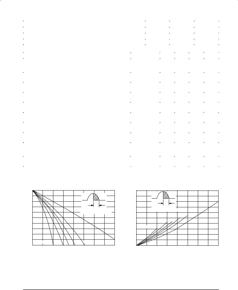
TYPICAL CHARACTERISTICS |
|
|
|
|
|
|
|
|||||
ALLOWABLE CASE TEMPERATURE (°C) |
125 |
|
|
|
|
|
|
|
|
|
AVERAGE ON-STATE POWER DISSIPATION |
|
15 |
|
|
|
|
|
|
|
|
115 |
|
|
|
|
|
|
|
α |
|
|
12 |
|
|
α |
|
|
|
|
|
||
|
|
|
|
|
|
|
|
|
|
|
|
|
|
|
|
|
|
|
|||
105 |
|
|
|
|
|
α = CONDUCTION ANGLE |
|
(WATTS) |
9 |
|
α = CONDUCTION ANGLE |
|
|
|
dc |
||||||
|
|
|
|
|
|
|
|
|
|
|
|
120° |
180° |
|
|
|
|||||
|
|
|
|
|
|
|
|
|
|
|
|
|
|
|
|
|
|||||
|
|
|
|
|
|
|
|
|
|
|
|
|
|
|
|
|
|
||||
95 |
|
|
|
|
|
|
|
|
|
|
|
|
60° |
90° |
|
|
|
|
|||
|
|
|
|
|
|
|
|
|
6 |
|
|
|
|
|
|
|
|||||
|
|
|
|
|
|
|
|
|
α = 30° |
|
|
|
|
|
|
||||||
|
|
|
|
|
|
|
|
|
|
|
|
|
|
|
|
|
|||||
85 |
|
|
|
|
|
|
|
dc |
|
|
|
|
|
|
|
|
|
|
|||
|
|
|
|
|
|
|
|
|
3 |
|
|
|
|
|
|
|
|
||||
|
|
|
|
|
|
|
|
|
|
|
|
|
|
|
|
|
|
|
|||
MAXIMUM, |
|
α = 30° |
|
60° |
90° |
120° |
180° |
|
|
|
, |
|
|
|
|
|
|
|
|
|
|
75 |
|
|
|
|
(AV) |
|
0 |
|
|
|
|
|
|
|
|
||||||
|
|
|
|
|
|
|
|
|
|
|
|
|
|
|
|
|
|
||||
C |
0 |
1 |
2 |
3 |
|
4 |
5 |
6 |
7 |
8 |
P |
|
0 |
1 |
2 |
3 |
4 |
5 |
6 |
7 |
8 |
T |
|
|
|||||||||||||||||||
|
|
IT(AV), AVERAGE ON-STATE FORWARD CURRENT (AMPS) |
|
|
|
|
|
IT(AV), AVG. ON-STATE CURRENT (AMPS) |
|
|
|||||||||||
Figure 1. Current Derating |
Figure 2. On-State Power Dissipation |
2 |
Motorola Thyristor Device Data |
 Loading...