


UCC5672PWPTR
UCC5672
SLUS414A - FEBRUARY 2000
FEATURES
•
Auto Selection Multi-Mode Single
Ended or Low Voltage Differential
Termination
•
2.7V to 5.25V Operation
•
Differential Failsafe Bias
•
Built-in SPI-3 Mode Change Filter/
Delay
•
Meets SCSI-1, SCSI-2, Ultra2 (SPI-2
LVD) and Ultra3/Ultra160 Standards
•
Supports Active Negation
•
3pF Channel Capacitance
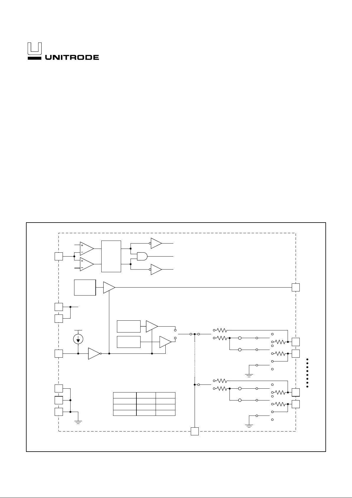
Multimode (LVD/SE) SCSI 9 Line Terminator
1
27
16 DIFSENS
DIFSENS
REF 1.3V
ENABLE
3L1–
52
2L1+
52
L9–
L9+
56mV
+–
56mV
–+
124
110
SE GROUND
SWITCH
26
52
25
52
56mV
+–
56mV
–+
124
110
SE GROUND
SWITCH
REG
17
DIFFB
0.6V
2.1V
FILTER/
DELAY
28TRMPWR
TRMPWR
LVD REF
1.25V
SOURCE/SINK
REGULATORS
SE REF
2.7V
ENABLE
SW1
10µA
22
6HS/GND
HS/GND
14GND
13DISCNCT
SE
DISCNCT
HPD
LVD
UP
OPEN
DOWN
DOWN DOWN
UP
OPEN
OPEN
MODE SW1
OTHER
SWITCHES
HPD
LVD
SE
BLOCK DIAGRAM
UDG-99125
DESCRIPTION
The UCC5672 Multi-Mode Low Voltage Differential and Single Ended Ter
-
minator is both a single ended terminator and a low voltage differential ter
-
minator for the transition to the next generation SCSI Parallel Interface
(SPI-3). The low voltage differential is a requirement for the higher speeds
at a reasonable cost and is the only way to have adequate skew budgets.
The automatic mode select/change feature switches the terminator be
-
tween Single Ended or LVD SCSI Termination, depending on the bus
mode. If the bus is in High Voltage Differential Mode, the terminator lines
transition into a High Impedance state.
The UCC5672 is SPI-3, SPI-2, and SCSI-2 compliant. This device is of
-
fered in a 28 pin TSSOP package to minimize the footprint. The UCC5672
is also available in a 36 pin MWP package.
Note: Indicated pinout is for 28 pin TSSOP package.
2
UCC5672
ABSOLUTE MAXIMUM RATINGS
TRMPWR Voltage . . . . . . . . . . . . . . . . . . . . . . . . . . . . . . . . . 6V
Signal Line Voltage . . . . . . . . . . . . . . . . . . . . . . . . . . . 0V to 5V
Storage Temperature . . . . . . . . . . . . . . . . . . . –65°C to +150°C
Junction Temperature. . . . . . . . . . . . . . . . . . . –55°C to +150°C
Lead Temperature (Soldering, 10sec.) . . . . . . . . . . . . . +300°C
All voltages are with respect to GND.Currents are positive into,
negative out of the specified terminal. Consult Packaging Sec
-
tion of the Databook for thermal limitations and considerations
of packages.
RECOMMENDED OPERATING CONDITIONS
TRMPWR Voltage . . . . . . . . . . . . . . . . . . . . . . . . 2.7V to 5.25V
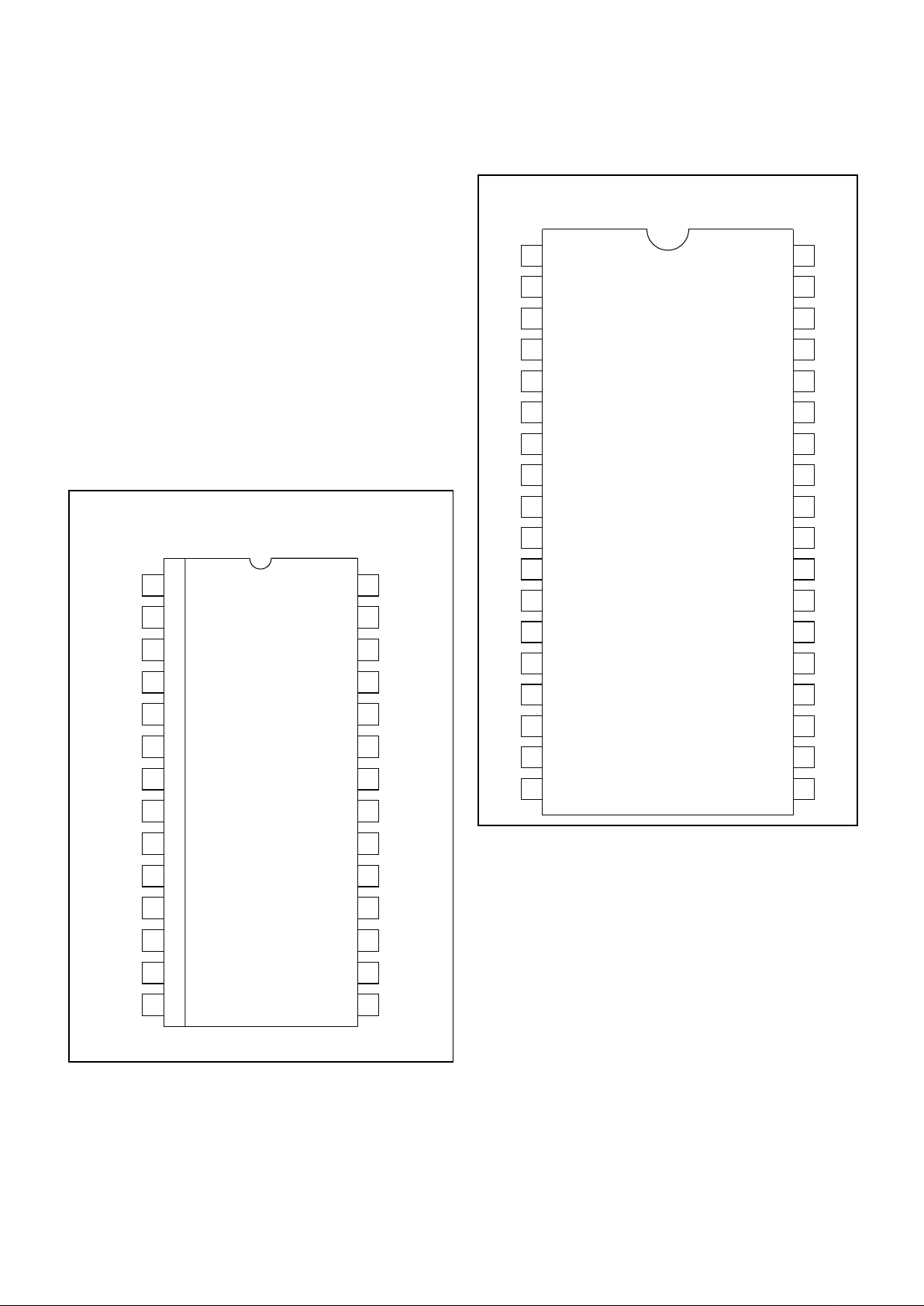
DIFFB
L6+
L8–
L8+
L7–
TRMPWR
L1+
L4–
L3+
L4+
L1–
L2+
L2–
REG
L3–
DIFSENS
L7+
L6–
L5+
GND 14
13
12
11
10
9
8
7
6
5
4
3
2
1
15
16
17
18
19
20
21
22
23
24
25
26
27
28
L5–
N/C
DISCNCT
L9–
L9+
TRMPWR
HS/GND
HS/GND
CONNECTION DIAGRAM
L3+
HS/GND
L9–
L9+
L8–
TRMPWR
N/C
N/C
HS/GND
L2–
HS/GND
L1+
L1–
L2+
REG
HS/GND
L3–
L8+
HS/GND
HS/GND
L4+
L4–
14
13
12
11
10
9
8
7
6
5
4
3
2
1
23
24
25
26
27
28
29
30
31
32
33
34
35
36
18
17
16
15
DIFF B
N/C
DIFSENS
19
20
21
22L5+
L5–
DISCNCT
GND
L7–
L7+
L6–
L6+
N/C
N/C
N/C
TSSOP-28 (TOP VIEW)
PWP Package
QSOP-36 (TOP VIEW)
MWP Package
 Loading...