


Texas Instruments UCC5640PWXTR, UCC5640PWX, UCC5640PW28TR, UCC5640PW24TR, UCC5640PW28 Datasheet
...
UCC5640
Low Voltage Differential (LVD) SCSI 9 Line Terminator
FEATURES
•First LVD only Active Terminator
•Meets SCSI SPI-2 Ultra2 (Fast-40) and Ultra3 / Ultra160 (Fast-80) Standards
•2.7V to 5.25V Operation
•Differential Failsafe Bias
DESCRIPTION
The UCC5640 is an active terminator for Low Voltage Differential (LVD) SCSI networks. This LVD only design allows the user to reach peak bus performance while reducing system cost. The device is designed as an active Y-terminator to improve the frequency response of the LVD Bus. Designed with a 1.5pF channel capacitance, the UCC5640 allows for minimal bus loading for a maximum number of peripherals. With the UCC5640, the designer will be able to comply with the Fast-40 SPI-2 and Fast-80 SPI-3 specifications. The UCC5640 also provides a much-needed system migration path for ever improving SCSI system standards. This device is available in the 24 pin TSSOP and 28 pin TSSOP for ease of layout use.
The UCC5640 is not designed for use in single ended or high voltage differential systems.
BLOCK DIAGRAM
SOURCE ONLY FROM TRMPWR AND THE ENABLED TERMINATIONS
|
|
|
|
|
|
SOURCE 5–15mA |
TRMPWR |
28 |
|
2.7V to 5.25V |
|
||
|
SINK 200 |
A MAXIMUM (NOISE LOAD) |
||||
|
|
|
|
|
||
REF 1.3V 
OPEN CIRCUIT ON POWER OFF OR OPEN CIRCUIT IN A DISABLED TERMINATOR MODE
12
|
|
1.3V ± 0.1V |
|
|
DIFSENS |
||
|
|
|
|
|
|
HIGH POWER |
|
|
|
2.4V > 1.9V |
|
|
|
DIFFERENTIAL |
|
|
|
|
|
|
|
|
|
20k |
DIFFB |
|
|
|
|
|
|
|
|
|
|
|
|
|
|
|
11 |
|
|
|
|
27 |
LVD* |
|
HIGH IMPEDANCE RECEIVER |
|
|
|
|
|
|
0.1 F |
EVEN WITH POWER OFF |
0.7V > 0.5V |
|
|
|
|
|
|
|
|
|
|
SINGLE |
|
|
|
|
|
|
|
|
|
|
|
|
|
|
|
|
ENDED |
|
|
SOURCE/SINK REGULATOR |
124 |
56mV |
|
|
||
|
|
|
52 |
|
|||
LOW |
REF 1.25V |
|
|
|
|||
|
|
– |
+ |
|
|||
|
|
4 |
L1– |
||||
FREQUENCY |
|
|
|
||||
|
|
|
|
|
|||
|
|
|
|
|
|
|
|
FILTER |
|
|
|
56mV |
52 |
|
|
50Hz – 60Hz |
|
|
|
|
|||
|
|
|
+ |
– |
|
||
10 A |
|
|
3 |
L1+ |
|||
|
|
|
|||||
|
|
|
|
|
|||
|
|
|
124 |
56mV |
52 |
|
|
|
|
|
|
|
|||
|
|
|
|
– |
+ |
|
|
|
|
|
|
26 |
L9– |
||
|
|
|
|
|
|
||
DISCNCT |
15 |
|
|
56mV |
52 |
|
|
|
|
|
|
|
|||
|
|
|
|
+ |
– |
|
|
|
|
|
|
25 |
L9+ |
||
|
|
|
|
|
|
||
|
GND |
REG |
|
|
|
|
|
|
14 |
1 |
|
|
|
|
|
|
|
4.7 F |
|
|
|
|
|
* 28 pin package only |
|
|
|
|
UDG-98181 |
||
|
|
|
|
|
|
||
SLUS314A - JANUARY 2000
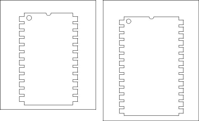
CONNECTION DIAGRAMS
TSSOP-24 (Top View)
PW24 Package
REG |
1 |
24 |
TRMPWR |
L1+ |
2 |
23 |
L9– |
L1– |
3 |
22 |
L9+ |
L2+ |
4 |
21 |
L8– |
L2– |
5 |
20 |
L8+ |
L3+ |
6 |
19 |
L7– |
L3– |
7 |
18 |
L7+ |
L4+ |
8 |
17 |
L6– |
L4– |
9 |
16 |
L6+ |
DIFFB |
10 |
15 |
L5– |
DIFSENS |
11 |
14 |
L5+ |
GND |
12 |
13 |
DISCNCT |
ABSOLUTE MAXIMUM RATINGS
UCC5640
TSSOP-28 (Top View)
PW28 Package
REG |
1 |
28 |
TRMPWR |
N/C |
2 |
27 |
LVD |
L1+ |
3 |
26 |
L9– |
L1– |
4 |
25 |
L9+ |
L2+ |
5 |
24 |
L8– |
L2– |
6 |
23 |
L8+ |
L3+ |
7 |
22 |
L7– |
L3– |
8 |
21 |
L7+ |
L4+ |
9 |
20 |
L6– |
L4– |
10 |
19 |
L6+ |
DIFFB |
11 |
18 |
L5– |
DIFSENS |
12 |
17 |
L5+ |
N/C |
13 |
16 |
N/C |
GND |
14 |
15 |
DISCNCT |
TERMPWR Voltage. . . . . . . . . . . . . . . . . . . . . . . . . . . . . . . +6V
Signal Line Voltage . . . . . . . . . . . . . . . . . . . . . . . . . . 0V to 3.6V
Package Dissipation . . . . . . . . . . . . . . . . . . . . . . . . . . . . . . . 1W
Storage Temperature . . . . . . . . . . . . . . . . . . . –65°C to +150°C
Junction Temperature. . . . . . . . . . . . . . . . . . . –55°C to +150°C
Lead Temperature (Soldering, 10 sec.) . . . . . . . . . . . . . +300°C
Currents are positive into negative out of the specified terminal. consult Packaging Section of Databook for thermal limitations and considerations of package.
RECOMMENDED OPERATING CONDITIONS
TERMPWR Voltage . . . . . . . . . . . . . . . . . . . . . . . 2.7V to 5.25V
ELECTRICAL CHARACTERISTICS: Unless otherwise stated, specifications apply for TA = 0°C to 70°C, TRMPWR = 3.3V. TA = TJ.
PARAMETER |
TEST CONDITIONS |
MIN |
TYP |
MAX |
UNITS |
TRMPWR Supply Current Section |
|
|
|
|
|
TRMPWR Supply Current |
No Load |
|
|
25 |
mA |
|
Disabled Terminator |
|
|
400 |
A |
TRMPWR Voltage |
|
2.7 |
|
5.25 |
V |
2
 Loading...