


UCC5673
Multimode (LVD/SE) SCSI 9 Line Terminator
FEATURES
•Auto Selection Multi-Mode Single Ended or Low Voltage Differential Termination
•2.7V to 5.25V Operation
•Differential Failsafe Bias
•Built-in SPI-3 Mode Change Filter/ Delay
•Meets SCSI-1, SCSI-2, Ultra2 (SPI-2 LVD) and Ultra3/Ultra160 Standards
•Supports Active Negation
•3pF Channel Capacitance
•Reversed Disconnect Polarity
DESCRIPTION
The UCC5673 Multi-Mode Low Voltage Differential and Single Ended Terminator is both a single ended terminator and a low voltage differential terminator for the transition to the next generation SCSI Parallel Interface (SPI-3). The low voltage differential is a requirement for the higher speeds at a reasonable cost and is the only way to have adequate skew budgets.
The automatic mode select/change feature switches the terminator between Single Ended or LVD Termination, depending on the bus mode. If the bus is in High Voltage Differential Mode, the terminator lines transition into a High Impedance state.
The UCC5673 is SPI-3, SPI-2, and SCSI-2 compliant. This device is offered in a 28 pin TSSOP package to minimize the footprint. The UCC5673 is also available in a 36 pin MWP package.
BLOCK DIAGRAM
2.1V |
|
HPD |
|
|
|
||
DIFFB 17 |
FILTER/ |
LVD |
|
DELAY |
|||
|
|
||
0.6V |
|
SE |
DIFSENS
REF 1.3V
TRMPWR |
28 |
TRMPWR |
27 |
10 A
DISCNCT 13
HS/GND |
6 |
HS/GND |
22 |
GND |
14 |
ENABLE |
|
|
|
|
|
SOURCE/SINK |
|
|
|
|
|
REGULATORS |
|
|
|
|
|
SE REF |
SW1 |
110 |
|
|
|
2.7V |
|
|
|
||
|
|
|
|
||
|
|
|
56mV |
52 |
|
LVD REF |
|
|
– |
+ |
|
|
124 |
|
|||
1.25V |
|
56mV |
52 |
||
|
|
|
|||
|
|
|
+ |
– |
|
|
|
|
|
||
ENABLE |
|
|
|
|
|
16 DIFSENS
3 L1–
2 L1+
|
|
|
SE GROUND |
|
|
|
||
|
|
|
SWITCH |
|
|
|
||
|
|
|
110 |
|
|
|
|
|
MODE |
SW1 |
OTHER |
|
56mV |
52 |
|
||
SWITCHES |
|
|
||||||
|
|
|
– |
+ |
26 |
L9– |
||
SE |
UP |
UP |
124 |
|||||
56mV |
||||||||
52 |
|
|||||||
LVD |
DOWN |
DOWN |
|
+ |
– |
|
||
|
25 |
L9+ |
||||||
HPD |
DOWN |
OPEN |
|
|
|
|||
|
|
|
|
|
||||
DISCNCT |
OPEN |
OPEN |
SE GROUND |
|
|
|
||
|
|
|
|
|
|
|||
|
|
|
SWITCH |
|
|
|
||
1
REG
Note: Indicated pinout is for 28 pin TSSOP package. |
UDG-99162 |
|
SLUS438 - FEBRUARY 2000
ABSOLUTE MAXIMUM RATINGS
TRMPWR Voltage . . . . . . . . . . . . . . . . . . . . . . . . . . . . . . . . . 6V Signal Line Voltage . . . . . . . . . . . . . . . . . . . . . . . . . . . 0V to 5V Storage Temperature . . . . . . . . . . . . . . . . . . . –65°C to +150°C Junction Temperature. . . . . . . . . . . . . . . . . . . –55°C to +150°C Lead Temperature (Soldering, 10sec.) . . . . . . . . . . . . . +300°C
All voltages are with respect to GND. Currents are positive into, negative out of the specified terminal. Consult Packaging Section of the Databook for thermal limitations and considerations of packages.
RECOMMENDED OPERATING CONDITIONS
TRMPWR Voltage . . . . . . . . . . . . . . . . . . . . . . . . 2.7V to 5.25V
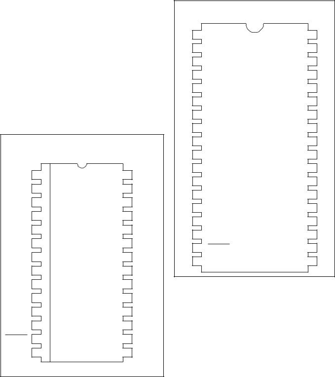
CONNECTION DIAGRAM
TSSOP-28 (TOP VIEW)
PWP Package
REG |
1 |
28 |
TRMPWR |
L1+ |
2 |
27 |
TRMPWR |
L1– |
3 |
26 |
L9– |
L2+ |
4 |
25 |
L9+ |
L2– |
5 |
24 |
L8– |
HS/GND |
6 |
23 |
L8+ |
L3+ |
7 |
22 |
HS/GND |
L3– |
8 |
21 |
L7– |
L4+ |
9 |
20 |
L7+ |
L4– |
10 |
19 |
L6– |
L5+ |
11 |
18 |
L6+ |
L5– |
12 |
17 |
DIFFB |
DISCNCT |
13 |
16 |
DIFSENS |
GND |
14 |
15 |
N/C |
UCC5673
QSOP-36 (TOP VIEW)
MWP Package
1 |
REG |
TRMPWR |
36 |
|
2 |
N/ |
N/ |
35 |
|
C |
C |
|||
|
|
|||
3 |
N/ |
N/ |
34 |
|
C |
C |
|||
|
|
|||
4 |
L1+ |
N/ |
33 |
|
C |
||||
|
|
|
||
5 |
L1– |
L9– |
32 |
|
6 |
L2+ |
L9+ |
31 |
|
7 |
L2– |
L8– |
30 |
|
8 |
HS/GND |
L8+ |
29 |
|
9 |
HS/GND |
HS/GND |
28 |
|
10 |
HS/GND |
HS/GND |
27 |
|
11 |
L3+ |
HS/GND |
26 |
|
12 |
L3– |
L7– |
25 |
|
13 |
L4+ |
L7+ |
24 |
|
14 |
L4– |
L6– |
23 |
|
15 |
L5+ |
L6+ |
22 |
|
16 |
L5– |
DIFF B |
21 |
|
17 |
DISCNCT |
DIFSENS |
20 |
|
18 |
GND |
N/C |
19 |
2

UCC5673
ELECTRICAL CHARACTERISTICS Unless otherwise stated, these specifications apply for TA = TJ = 0°C to 70°C, TRMPWR = 2.7V to 5.25V.
|
|
|
PARAMETER |
|
|
|
TEST CONDITIONS |
MIN |
TYP |
MAX |
UNITS |
|||
TRMPWR Supply Current Section |
|
|
|
|
|
|
|
|
|
|||||
|
TRMPWR Supply Current |
|
LVD Mode |
|
|
|
23 |
35 |
mA |
|||||
|
|
|
|
|
|
SE Mode |
|
|
|
14 |
25 |
mA |
||
|
|
|
|
|
|
|
|
|
|
|
|
|
|
µ A |
|
|
|
|
|
|
DISCNCT Mode |
|
|
|
250 |
500 |
|||
Regulator Section |
|
|
|
|
|
|
|
|
|
|||||
|
1.25V Regulator Output Voltage |
|
LVD Mode |
|
|
1.15 |
1.25 |
1.35 |
V |
|||||
|
1.25V Regulator Source Current |
|
VREG= 0V |
|
|
–800 |
–420 |
–225 |
mA |
|||||
|
1.25V Regulator Sink Current |
|
VREG= 3.3V |
|
|
100 |
180 |
420 |
mA |
|||||
|
2.7V Regulator Output Voltage |
|
SE Mode |
|
|
2.5 |
2.7 |
3.0 |
V |
|||||
|
2.7V Regulator Source Current |
|
VREG= 0V |
|
|
–800 |
–420 |
–225 |
mA |
|||||
|
2.7V Regulator Sink Current |
|
VREG= 3.3V |
|
|
100 |
180 |
420 |
mA |
|||||
Diff Sense Driver (DIFSENS) Section |
|
|
|
|
|
|
|
|
|
|||||
|
1.3V DIFSENS Output Voltage |
|
DIFSENS |
|
|
1.2 |
1.3 |
1.4 |
V |
|||||
|
1.3V DIFSENS Source Current |
|
VDIFSENS = 0V |
|
|
–15 |
|
–5 |
mA |
|||||
|
1.3V DIFSENS Sink Current |
|
VDIFSENS = 2.75V |
|
|
50 |
|
200 |
µ A |
|||||
Differential Termination Section |
|
|
|
|
|
|
|
|
|
|||||
|
Differential Impedance |
|
|
|
|
|
|
100 |
105 |
110 |
Ω |
|||
|
Common Mode Impedance |
|
(Note 2) |
|
|
110 |
150 |
165 |
Ω |
|||||
|
Differential Bias Voltage |
|
|
|
|
|
|
100 |
|
125 |
mV |
|||
|
Common Mode Bias |
|
|
|
|
|
|
1.15 |
1.25 |
1.35 |
V |
|||
|
Output Capacitance |
|
Single Ended Measurement to Ground (Note 1) |
|
|
3 |
pF |
|||||||
Single Ended Termination Section |
|
|
|
|
|
|
|
|
|
|||||
|
Impedance |
|
Z = |
(VLX − 0 . 2V ) |
|
, (Note 3) |
100 |
108 |
116 |
Ω |
||||
|
|
|
|
|
|
IL |
|
|
|
|
||||
|
|
|
|
|
|
|
|
|
|
|
|
|||
|
|
|
|
|
|
|
|
|
|
X |
|
|
|
|
|
|
|
|
|
|
|
|
|||||||
|
Termination Current |
|
Signal Level 0.2V, All Lines Low |
–25.4 |
–23 |
–20 |
mA |
|||||||
|
|
|
|
|
|
Signal Level 0.5V |
|
|
–22.4 |
|
–17 |
mA |
||
|
Output Leakage |
|
|
|
|
|
|
|
|
400 |
nA |
|||
|
Output Capacitance |
|
Single Ended Measurement to Ground (Note 1) |
|
|
3 |
pF |
|||||||
|
Single Ended GND SE Impedance |
|
I = 10mA |
|
|
|
20 |
60 |
Ω |
|||||
|
|
|
|
|
|
|
|
|
|
|
|
|
|
|
Disconnect (DISCNCT) and Diff Buffer (DIFFB) Input Section |
|
|
|
|
|
|
||||||||
|
DISCNCT Threshold |
|
|
|
|
|
|
0.8 |
|
2.0 |
V |
|||
|
|
|
|
|
|
|
|
|
|
|
|
|
|
µ A |
|
DISCNCT Input Current |
|
|
|
|
|
|
–30 |
–10 |
|
||||
|
DIFFB SE to LVD Threshold |
|
|
|
|
|
|
0.5 |
|
0.7 |
V |
|||
|
DIFFB LVD to HPD Threshold |
|
|
|
|
|
|
1.9 |
|
2.4 |
V |
|||
|
DIFFB Input Current |
|
|
|
|
|
|
–1 |
|
1 |
µ A |
|||
3
 Loading...