


ULN2001A, ULN2002A, ULN2003A, ULN2004A
DARLINGTON TRANSISTOR ARRAYS
SLRS027 ± DECEMBER 1976 ± REVISED APRIL 1993
HIGH-VOLTAGE HIGH-CURRENT DARLINGTON TRANSISTOR ARRAYS
D500-mA Rated Collector Current (Single Output)
DHigh-Voltage Outputs . . . 50 V
DOutput Clamp Diodes
DInputs Compatible With Various Types of Logic
DRelay Driver Applications
DDesigned to Be Interchangeable With Sprague ULN2001A Series
description
D OR N PACKAGE
(TOP VIEW)
1B |
|
1 |
16 |
|
1C |
|
|
||||
2B |
|
2 |
15 |
|
2C |
|
|
||||
3B |
|
3 |
14 |
|
3C |
|
|
||||
4B |
|
4 |
13 |
|
4C |
|
|
||||
5B |
|
5 |
12 |
|
5C |
|
|
||||
6B |
|
6 |
11 |
|
6C |
|
|
||||
7B |
|
7 |
10 |
|
7C |
|
|
||||
E |
|
8 |
9 |
|
COM |
|
|
||||
|
|
|
|
|
|
The ULN2001A, ULN2002A, ULN2003A, and ULN2004A are monolithic high-voltage, high-current Darlington transistor arrays. Each consists of seven npn Darlington pairs that feature high-voltage outputs with common-cathode clamp diodes for switching inductive loads. The collector-current rating of a single Darlington pair is 500 mA. The Darlington pairs may be paralleled for higher current capability. Applications include relay drivers, hammer drivers, lamp drivers, display drivers (LED and gas discharge), line drivers, and logic buffers. For 100-V (otherwise interchangeable) versions, see the SN75465 through SN75469.
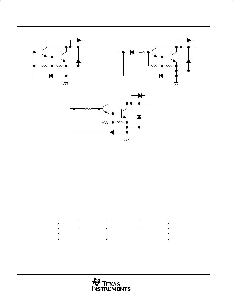
The ULN2001A is a general-purpose array and can be used with TTL and CMOS technologies. The ULN2002A is specifically designed for use with 14to 25-V PMOS devices. Each input of this device has a zener diode and resistor in series to control the input current to a safe limit. The ULN2003A has a 2.7-kΩ series base resistor for each Darlington pair for operation directly with TTL or 5-V CMOS devices. The ULN2004A has a 10.5-kΩ series base resistor to allow its operation directly from CMOS devices that use supply voltages of 6 to 15 V. The required input current of the ULN2004A is below that of the ULN2003A, and the required voltage is less than that required by the ULN2002A.
logic symbol² |
|
logic diagram |
|
|
|
9 |
|
9 |
|
CLAMP |
1 |
COM |
||
COM |
16 |
|||
|
|
1B |
1C |
|
1 |
16 |
|
|
|
1B |
1C |
2 |
15 |
|
2 |
15 |
|||
2B |
2C |
|||
2B |
2C |
|||
|
|
|||
3 |
14 |
|
|
|
3B |
3C |
3 |
14 |
|
4 |
13 |
|||
3B |
3C |
|||
4B |
4C |
|||
|
|
|||
5 |
12 |
|
|
|
5B |
5C |
4 |
13 |
|
6 |
11 |
|||
4B |
4C |
|||
6B |
6C |
|||
|
|
|||
7 |
10 |
|
|
|
7B |
7C |
5 |
12 |
|
² This symbol is in accordance with ANSI/IEEE Std 91-1984 |
5B |
5C |
||
|
|
|||
and IEC Publication 617-12. |
|
6 |
11 |
|
|
|
6B |
6C |
|
|
|
7 |
10 |
|
|
|
7B |
7C |
|
PRODUCTION DATA information is current as of publication date. Products conform to specifications per the terms of Texas Instruments standard warranty. Production processing does not necessarily include testing of all parameters.
Copyright 1993, Texas Instruments Incorporated
POST OFFICE BOX 655303 •DALLAS, TEXAS 75265 |
1 |
ULN2001A, ULN2002A, ULN2003A, ULN2004A DARLINGTON TRANSISTOR ARRAYS
SLRS027 ± DECEMBER 1976 ± REVISED APRIL 1993
schematics (each Darlington pair)
Input B |
|
7.2 kΩ |
3 kΩ |
COM |
|
COM |
Output C |
7 V |
|
|
Output C |
|
|
|
|
Input B |
10.5 kΩ |
|
|
7.2 kΩ |
|
E |
|
|
|
3 kΩ |
E |
ULN2001A |
|
ULN2002A |
|
|
COM |
|
RB |
Output C |
|
|
|
Input B |
|
|
ULN2003A: RB = 2.7 kΩ |
|
|
ULN2004A: RB = 10.5 kΩ |
7.2 kΩ 3 kΩ |
E |
ULN2003A, ULN2004A
All resistor values shown are nominal.
absolute maximum ratings at 25°C free-air temperature (unless otherwise noted)
Collector-emitter voltage . . . . . . . . . . . . . . . . . . . . . . . . . . . . . . . . . . . . . . . . . . . . . . . |
. . . . . . . . . . . . . . . . . . . . . 50 V |
Input voltage, VI (see Note 1) . . . . . . . . . . . . . . . . . . . . . . . . . . . . . . . . . . . . . . . . . . . |
. . . . . . . . . . . . . . . . . . . . . 30 V |
Peak collector current (see Figures 14 and 15) . . . . . . . . . . . . . . . . . . . . . . . . . . . |
. . . . . . . . . . . . . . . . . . 500 mA |
Output clamp current, IOK . . . . . . . . . . . . . . . . . . . . . . . . . . . . . . . . . . . . . . . . . . . . . . |
. . . . . . . . . . . . . . . . . . 500 mA |
Total emitter-terminal current . . . . . . . . . . . . . . . . . . . . . . . . . . . . . . . . . . . . . . . . . . . |
. . . . . . . . . . . . . . . . . . . ±2.5 A |
Continuous total power dissipation . . . . . . . . . . . . . . . . . . . . . . . . . . . . . . . . . . . . . |
See Dissipation Rating Table |
Operating free-air temperature range, TA . . . . . . . . . . . . . . . . . . . . . . . . . . . . . . . . |
. . . . . . . . . . . . ±20°C to 85°C |
Storage temperature range, Tstg . . . . . . . . . . . . . . . . . . . . . . . . . . . . . . . . . . . . . . . . |
. . . . . . . . . . . ±65°C to 150°C |
Lead temperature 1,6 mm (1/16 inch) from case for 10 seconds . . . . . . . . . . . . |
. . . . . . . . . . . . . . . . . . . 260°C |
NOTE 1: All voltage values are with respect to the emitter/substrate terminal E, unless otherwise noted.
DISSIPATION RATING TABLE
PACKAGE |
TA = 25°C |
DERATING FACTOR |
TA = 85°C |
|
POWER RATING |
ABOVE TA = 25°C |
POWER RATING |
||
|
||||
D |
950 mW |
7.6 mW/°C |
494 mW |
|
N |
1150 mW |
9.2 mW/°C |
598 mW |
|
|
|
|
|
2 |
POST OFFICE BOX 655303 •DALLAS, TEXAS 75265 |
ULN2001A, ULN2002A, ULN2003A, ULN2004A
DARLINGTON TRANSISTOR ARRAYS
SLRS027 ± DECEMBER 1976 ± REVISED APRIL 1993
electrical characteristics, TA = 25°C (unless otherwise noted)
|
PARAMETER |
TEST |
TEST CONDITIONS |
ULN2001A |
|
ULN2002A |
|
UNIT |
|||
|
FIGURE |
MIN |
TYP |
MAX |
MIN |
TYP |
MAX |
||||
|
|
|
|
|
|||||||
|
|
|
|
|
|
|
|
|
|
|
|
VI(on) |
On-state input voltage |
6 |
VCE = 2 V, |
IC = 300 mA |
|
|
|
|
|
13 |
V |
|
Collector-emitter |
|
II = 250 A, |
IC = 100 mA |
|
0.9 |
1.1 |
|
0.9 |
1.1 |
|
VCE(sat) |
5 |
II = 350 A, |
IC = 200 mA |
|
1 |
1.3 |
|
1 |
1.3 |
V |
|
saturation voltage |
|
|
|||||||||
|
|
|
II = 500 A, |
IC = 350 mA |
|
1.2 |
1.6 |
|
1.2 |
1.6 |
|
VF |
Clamp forward voltage |
8 |
IF = 350 mA |
|
|
1.7 |
2 |
|
1.7 |
2 |
V |
|
|
1 |
VCE = 50 V, |
II = 0 |
|
|
50 |
|
|
50 |
|
ICEX |
Collector cutoff current |
2 |
VCE = 50 V, |
II = 0 |
|
|
100 |
|
|
100 |
A |
|
|
TA = 70°C |
V = 6 V |
|
|
|
|
|
500 |
|
|
|
|
|
|
|
|
|
|
|
|||
|
|
|
|
I |
|
|
|
|
|
|
|
II(off) |
Off-state input current |
3 |
VCE = 50 V, |
IC = 500 A, |
50 |
65 |
|
50 |
65 |
|
A |
TA = 70°C |
|
|
|
||||||||
|
|
|
|
|
|
|
|
|
|
|
|
II |
Input current |
4 |
VI = 17 V |
|
|
|
|
|
0.82 |
1.25 |
mA |
IR |
Clamp reverse current |
7 |
VR = 50 V, |
TA = 70°C |
|
|
100 |
|
|
100 |
A |
VR = 50 V |
|
|
|
50 |
|
|
50 |
||||
|
|
|
|
|
|
|
|
|
|||
hFE |
Static forward current |
5 |
VCE = 2 V, |
IC = 350 mA |
1000 |
|
|
|
|
|
|
transfer ratio |
|
|
|
|
|
|
|||||
|
|
|
|
|
|
|
|
|
|
|
|
|
|
|
|
|
|
|
|
|
|
|
|
Ci |
Input capacitance |
|
VI = 0, |
f = 1 MHz |
|
15 |
25 |
|
15 |
25 |
pF |
electrical characteristics, TA = 25°C (unless otherwise noted)
|
PARAMETER |
TEST |
TEST CONDITIONS |
ULN2003A |
|
ULN2004A |
|
UNIT |
|
|||
|
FIGURE |
MIN |
TYP |
MAX |
MIN |
TYP |
MAX |
|
||||
|
|
|
|
|
|
|||||||
|
|
|
|
|
|
|
|
|
|
|
|
|
|
|
|
|
IC = 125 mA |
|
|
|
|
|
5 |
|
|
|
|
|
|
IC = 200 mA |
|
|
2.4 |
|
|
6 |
|
|
VI(on) |
On-state input voltage |
6 |
VCE = 2 V |
IC = 250 mA |
|
|
2.7 |
|
|
|
V |
|
IC = 275 mA |
|
|
|
|
|
7 |
|
|||||
|
|
|
|
|
|
|
|
|
|
|
||
|
|
|
|
IC = 300 mA |
|
|
3 |
|
|
|
|
|
|
|
|
|
IC = 350 mA |
|
|
|
|
|
8 |
|
|
|
Collector-emitter |
|
II = 250 A, |
IC = 100 mA |
|
0.9 |
1.1 |
|
0.9 |
1.1 |
|
|
VCE(sat) |
5 |
II = 350 A, |
IC = 200 mA |
|
1 |
1.3 |
|
1 |
1.3 |
V |
|
|
saturation voltage |
|
|
|
|||||||||
|
|
|
II = 500 A, |
IC = 350 mA |
|
1.2 |
1.6 |
|
1.2 |
1.6 |
|
|
|
|
1 |
VCE = 50 V, |
II = 0 |
|
|
50 |
|
|
50 |
|
|
ICEX |
Collector cutoff current |
2 |
VCE = 50 V, |
II = 0 |
|
|
100 |
|
|
100 |
A |
|
|
|
TA = 70°C |
V = 1 V |
|
|
|
|
|
500 |
|
|
|
|
|
|
|
|
|
|
|
|
|
|||
|
|
|
|
I |
|
|
|
|
|
|
|
|
VF |
Clamp forward voltage |
8 |
IF = 350 mA |
|
|
1.7 |
2 |
|
1.7 |
2 |
V |
|
II(off) |
Off-state input current |
3 |
VCE = 50 V, |
IC = 500 A, |
50 |
65 |
|
50 |
65 |
|
A |
|
TA = 70°C |
|
|
|
|
||||||||
|
|
|
|
|
|
|
|
|
|
|
|
|
|
|
|
VI = 3.85 V |
|
|
0.93 |
1.35 |
|
|
|
|
|
II |
Input current |
4 |
VI = 5 V |
|
|
|
|
|
0.35 |
0.5 |
mA |
|
|
|
|
VI = 12 V |
|
|
|
|
|
1 |
1.45 |
|
|
IR |
Clamp reverse current |
7 |
VR = 50 V |
|
|
|
50 |
|
|
50 |
A |
|
VR = 50 V, |
TA = 70°C |
|
|
100 |
|
|
100 |
|
||||
|
|
|
|
|
|
|
|
|
||||
Ci |
Input capacitance |
|
VI = 0, |
f = 1 MHz |
|
15 |
25 |
|
15 |
25 |
pF |
|
|
|
|
|
|
|
|
|
|
|
|
|
|
|
|
|
|
|
|
|
|
|
|
|
|
|
POST OFFICE BOX 655303 •DALLAS, TEXAS 75265 |
3 |
 Loading...