


MC74LVX157DTR2
SEMICONDUCTOR TECHNICAL DATA
1
REV 0
Motorola, Inc. 1997
6/97
!
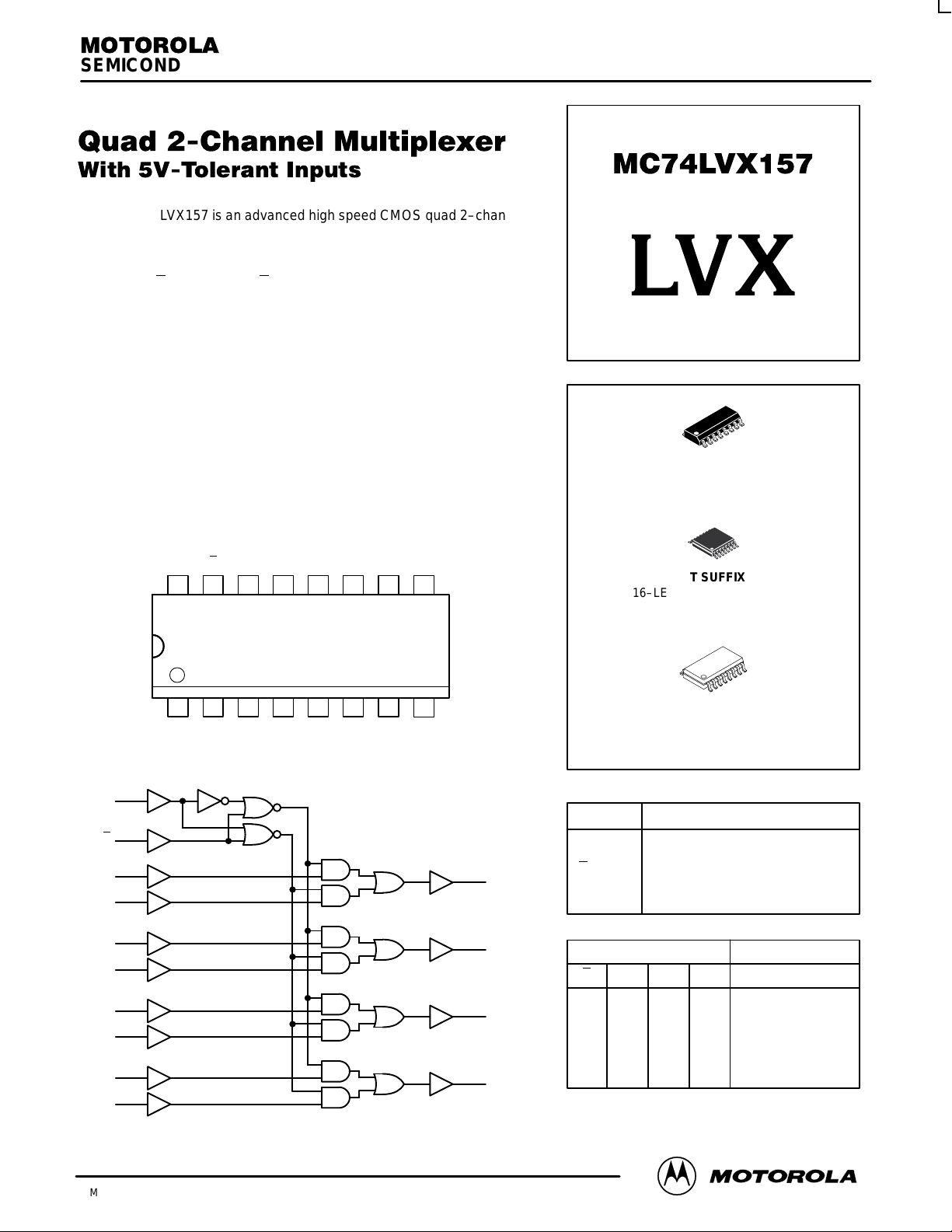
The MC74L VX157 is an advanced high speed CMOS quad 2–channel
multiplexer. The inputs tolerate voltages up to 7V, allowing the interface of
5V systems to 3V systems.
It consists of four 2–input digital multiplexers with common select (S)
and enable (E
) inputs. When E is held High, selection of data is inhibited
and all the outputs go Low.
The select decoding determines whether the I0n or I1n inputs get
routed to the corresponding Zn outputs.
• High Speed: t
PD
= 5.1ns (Typ) at V
CC
= 3.3V
• Low Power Dissipation: I
CC
= 4µA (Max) at T
A
= 25°C
• Power Down Protection Provided on Inputs
• Balanced Propagation Delays
• Low Noise: V
OLP
= 0.5V (Max)
• Pin and Function Compatible with Other Standard Logic Families
• Latchup Performance Exceeds 300mA
• ESD Performance: HBM > 2000V; Machine Model > 200V
1516 14 13 12 11 10
21 34567
V
CC
9
8
E
I0c I1c Zc I0d I1d Zd
S I0a I1a Za I0b I1b Zb GND
Figure 1. 16–Lead Pinout (Top View)
Za
I0a
4
2
E
I1a
3
15
Zb
I0b
7
5
I1b
6
Zc
I0c
12
14
I1c
13
Zd
I0d
9
11
I1d
10
S
1
Figure 2. Logic Diagram
LVX
LOW–VOLTAGE CMOS
D SUFFIX
16–LEAD SOIC PACKAGE
CASE 751B–05
DT SUFFIX
16–LEAD TSSOP PACKAGE
CASE 948F–01
M SUFFIX
16–LEAD SOIC EIAJ PACKAGE
CASE 966–01
H
L
L
L
L
INPUTS OUTPUT
E
L
L
H
L
H
Zn
TRUTH TABLE
PIN NAMES
Function
Source 0 Data Inputs
Source 1 Data Inputs
Enable Input
Select Input
Outputs
Pins
I0n
I1n
E
S
Zn
X
H
H
L
L
S
X
X
X
L
H
I0n
X
L
H
X
X
I1n
H = High Voltage Level; L = Low Voltage Level; X = High or Low
Voltage Level ; For I
CC
Reasons DO NOT FLOAT Inputs
MC74LVX157
MOTOROLA LCX DATA
BR1339 — REV 3
2
MAXIMUM RATINGS*
Symbol
Parameter
Value
Unit
V
CC
DC Supply Voltage
–0.5 to +7.0
V
V
in
DC Input Voltage
–0.5 to +7.0
V
V
out
DC Output Voltage
–0.5 to V
CC
+0.5
V
I
IK
Input Diode Current
–20
mA
I
OK
Output Diode Current
±20
mA
I
out
DC Output Current, per Pin
±25
mA
I
CC
DC Supply Current, V
CC
and GND Pins
±50
mA
P
D
Power Dissipation
180
mW
T
stg
Storage Temperature
–65 to +150
_
C
* Absolute maximum continuous ratings are those values beyond which damage to the device may occur. Exposure to these conditions or
conditions beyond those indicated may adversely affect device reliability. Functional operation under absolute–maximum–rated conditions is
not implied.
RECOMMENDED OPERATING CONDITIONS
Symbol
Parameter
Min
Max
Unit
V
CC
DC Supply Voltage
2.0
3.6
V
V
in
DC Input Voltage
0
5.5
V
V
out
DC Output Voltage
0
V
CC
V
T
A
Operating Temperature, All Package Types
–40
+85
_
C
∆t/∆V
Input Rise and Fall Time
0
100
ns/V
DC ELECTRICAL CHARACTERISTICS
ОООООО
V
T
A
= 25°C
T
A
= – 40 to 85°C
Symbol
Parameter
ОООООО
Test Conditions
V
CC
V
Min
Typ
Max
Min
Max
Unit
ÎÎ
Î
V
IH
ОООООО
Î
High–Level Input Voltage
ОООООО
ООООО
Î
Î
Î
2.0
3.0
3.6
ÎÎ
Î
1.5
2.0
2.4
Î
Î
ÎÎ
Î
ÎÎ
Î
1.5
2.0
2.4
ÎÎ
Î
Î
V
ÎÎ
Î
V
IL
ОООООО
Î
Low–Level Input Voltage
ОООООО
ООООО
Î
Î
Î
2.0
3.0
3.6
ÎÎ
Î
Î
Î
ÎÎ
Î
0.5
0.8
0.8
ÎÎ
Î
ÎÎ
Î
0.5
0.8
0.8
Î
V
ÎÎ
Î
ÎÎ
Î
V
OH
ОООООО
Î
ОООООО
Î
High–Level Output Voltage
(V
in
= V
IH
or V
IL
)
ОООООО
ООООО
Î
ООООО
Î
I
OH
= –50µA
I
OH
= –50µA
I
OH
= –4mA
Î
Î
Î
Î
2.0
3.0
3.0
ÎÎ
Î
ÎÎ
Î
1.9
2.9
2.58
Î
Î
Î
Î
2.0
3.0
ÎÎ
Î
ÎÎ
Î
ÎÎ
Î
ÎÎ
Î
1.9
2.9
2.48
ÎÎ
Î
ÎÎ
Î
Î
Î
V
ÎÎ
Î
V
OL
ОООООО
Î
Low–Level Output Voltage
(V
in
= V
IH
or V
IL
)
ОООООО
ООООО
Î
I
OL
= 50µA
I
OL
= 50µA
I
OL
= 4mA
Î
Î
2.0
3.0
3.0
ÎÎ
Î
Î
Î
0.0
0.0
ÎÎ
Î
0.1
0.1
0.36
ÎÎ
Î
ÎÎ
Î
0.1
0.1
0.44
Î
V
I
in
Input Leakage Current
ОООООО
V
in
= 5.5V or GND
3.6
±0.1
±1.0
µA
I
CC
Quiescent Supply Current
ОООООО
V
in
= V
CC
or GND
3.6
4.0
40.0
µA
 Loading...