


 Loading...
WL1801MOD, WL1805MOD, WL1831MOD, WL1835MOD
WL1801MOD, WL1805MOD, WL1831MOD, WL1835MOD
SWRS152N – JUNE 20 3 – REVISED APRIL 2021
SWRS152N – JUNE 2013 – REVISED APRIL 2021
WL18x1MOD, WL18x5MOD WiLink™ 8 Single-Band Combo Module – Wi-Fi®, Bluetooth ®, and Bluetooth Low Energy (LE)
1 Features
•General
–Integrates RF, power amplifiers (PAs), clock, RF switches, filters, passives, and power management
–Quick hardware design with TI module collateral and reference designs
–Operating temperature: –20°C to +70°C
–Small form factor: 13.3 × 13.4 × 2 mm
–100-pin MOC package
–FCC, IC, ETSI/CE, and TELEC certified with PCB, dipole, chip, and PIFA antennas
•Wi-Fi®
–WLAN baseband processor and RF transceiver support of IEEE Std 802.11b, 802.11g, and 802.11n
–20and 40-MHz SISO and 20-MHz 2 × 2 MIMO at 2.4 GHz for high throughput: 80 Mbps (TCP), 100 Mbps (UDP)
–2.4-GHz MRC support for extended range
–Fully calibrated: production calibration not required
–4-bit SDIO host interface support
–Wi-Fi direct concurrent operation (multichannel, multirole)
•Bluetooth® and Bluetooth low energy (WL183xMOD only)
–Bluetooth 5.1 secure connection compliant and CSA2 support (declaration ID: D032799)
–Host controller interface (HCI) transport for Bluetooth over UART
–Dedicated audio processor support of SBC encoding + A2DP
–Dual-mode Bluetooth and Bluetooth low energy
–TI's Bluetooth and Bluetooth low energy certified stack
•Key benefits
–Reduces design overhead
–Differentiated use cases by configuring WiLink™ 8 simultaneously in two roles (STA and AP) to connect directly with other WiFi devices on different RF channel (Wi-Fi networks)
–Best-in-class Wi-Fi with high-performance audio and video streaming reference applications with up to 1.4× the range versus one antenna
–Different provisioning methods for in-home devices connectivity to Wi-Fi in one step
–Lowest Wi-Fi power consumption in connected idle (< 800 µA)
–Configurable wake on WLAN filters to only wake up the system
–Wi-Fi and Bluetooth single antenna coexistence
2 Applications
•Internet of things (IoT)
•Multimedia
•Home electronics
•Home appliances and white goods
•Industrial and home automation
•Smart gateway and metering
•Video conferencing
•Video camera and security
3 Description
The certified WiLink™ 8 module from TI offers high throughput and extended range along with Wi-Fi® and Bluetooth® coexistence (WL1835MOD only) in a power-optimized design. The WL18x5MOD device is a 2.4-GHz module, two antenna solution. The device is FCC, IC, ETSI/CE, and TELEC certified for AP and client. TI offers drivers for high-level operating systems such as Linux® and Android™. Additional drivers, such as WinCE and RTOS, which includes QNX, Nucleus, ThreadX, and FreeRTOS, are supported through third parties.
Device Information(1)
PART NUMBER |
PACKAGE |
BODY SIZE |
WL1801MOD |
QFM (100) |
13.3 mm × 13.4 mm × 2 mm |
|
|
|
WL1805MOD |
QFM (100) |
13.3 mm × 13.4 mm × 2 mm |
|
|
|
WL1831MOD |
QFM (100) |
13.3 mm × 13.4 mm × 2 mm |
|
|
|
WL1835MOD |
QFM (100) |
13.3 mm × 13.4 mm × 2 mm |
|
|
|
(1)For more information, see Section 12.
An©IMPORTANT2021 Texas InstrumentsNOTICEIncorporatedthe end of this data sheet addresses availability, warranty, changes, use in safety-critical applications, |
1 |
Submit Document Feedback |
intellectual property matters and other important disclaimers. PRODUCTION DATA.
Product Folder Links: WL1801MOD WL1805MOD WL1831MOD WL1835MOD
WL1801MOD, WL1805MOD, WL1831MOD, WL1835MOD
SWRS152N – JUNE 2013 – REVISED APRIL 2021 |
www.ti.com |
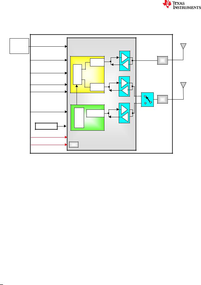
4 Functional Block Diagram
Figure 4-1 shows a functional block diagram of the WL1835MOD variant.
ZigBee |
|
|
|
|
RF_ANT2 |
|
|
|
|
|
|
COEX |
|
|
|
BG1 |
|
Interface |
|
|
|
|
|
|
|
|
|
|
|
BT_UART |
|
|
WRF2 |
|
F |
|
|
|
|
|
|
WLAN_SDIO |
|
<![if ! IE]> <![endif]>MAC/PHY |
|
BG2 |
|
|
|
|
|
||
|
|
|
|
RF_ANT1 |
|
|
|
|
|
|
|
BT_EN |
|
|
WRF1 |
|
2.4-GHz |
|
|
|
|
||
WLAN_EN |
|
|
|
|
SPDT |
|
|
|
|
|
|
|
|
|
|
BT |
F |
|
|
|
|
|
|
32.768 kHz |
|
<![if ! IE]> <![endif]>MAC/PHY |
BTRF |
|
|
|
|
|
|
||
|
26M XTAL |
|
|
|
|
|
|
|
|
|
|
VIO |
|
|
|
|
|
VBAT |
|
PM |
|
|
|
Copyright © 2017, Texas Instruments Incorporated
NOTE: Dashed lines indicate optional configurations and are not applied by default.
Figure 4-1. WL1835MOD Functional Block Diagram
2 |
Submit Document Feedback |
Copyright © 2021 Texas Instruments Incorporated |
|
Product Folder Links: WL1801MOD WL1805MOD WL1831MOD WL1835MOD |
|

www.ti.com |
WL1801MOD, WL1805MOD, WL1831MOD, WL1835MOD |
SWRS152N – JUNE 2013 – REVISED APRIL 2021 |
Table of Contents
1 |
Features............................................................................ |
1 |
|
2 |
Applications..................................................................... |
1 |
|
3 |
Description....................................................................... |
1 |
|
4 |
Functional Block Diagram.............................................. |
2 |
|
5 |
Revision History.............................................................. |
3 |
|
6 Device Comparison......................................................... |
4 |
||
|
6.1 |
Related Products........................................................ |
4 |
7 |
Terminal Configuration and Functions.......................... |
5 |
|
|
7.1 |
Pin Attributes............................................................... |
6 |
8 |
Specifications.................................................................. |
9 |
|
|
8.1 |
Absolute Maximum Ratings........................................ |
9 |
|
8.2 |
ESD Ratings............................................................... |
9 |
|
8.3 |
Recommended Operating Conditions......................... |
9 |
|
8.4 |
External Digital Slow Clock Requirements................ |
10 |
|
8.5 |
Thermal Resistance Characteristics for MOC |
|
|
100-Pin Package......................................................... |
10 |
|
|
8.6 |
WLAN Performance: 2.4-GHz Receiver |
|
|
Characteristics............................................................. |
11 |
|
|
8.7 |
WLAN Performance: 2.4-GHz Transmitter Power.... |
12 |
|
8.8 |
WLAN Performance: Currents.................................. |
13 |
|
8.9 |
Bluetooth Performance: BR, EDR Receiver |
|
|
Characteristics—In-Band Signals................................ |
13 |
|
|
8.10 Bluetooth Performance: Transmitter, BR ............... |
15 |
|
|
8.11 Bluetooth Performance: Transmitter, EDR.............. |
15 |
|
|
8.12 Bluetooth Performance: Modulation, BR................. |
15 |
|
|
8.13 Bluetooth Performance: Modulation, EDR.............. |
16 |
|
|
8.14 Bluetooth low energy Performance: Receiver |
|
|
|
Characteristics – In-Band Signals............................... |
16 |
|
|
8.15 Bluetooth low energy Performance: Transmitter |
|
|
|
Characteristics............................................................. |
16 |
|
8.16 |
Bluetooth low energy Performance: Modulation |
|
|
Characteristics............................................................. |
17 |
||
8.17 |
Bluetooth BR and EDR Dynamic Currents............. |
17 |
|
8.18 |
Bluetooth low energy Currents................................ |
17 |
|
8.19 |
Timing and Switching Characteristics..................... |
18 |
|
9 Detailed Description...................................................... |
26 |
||
9.1 |
WLAN Features........................................................ |
27 |
|
9.2 |
Bluetooth Features.................................................... |
27 |
|
9.3 |
Bluetooth Low Energy Features................................ |
28 |
|
9.4 |
Device Certification................................................... |
28 |
|
9.5 |
Module Markings....................................................... |
30 |
|
9.6 |
Test Grades............................................................... |
30 |
|
9.7 |
End Product Labeling................................................ |
31 |
|
9.8 |
Manual Information to the End User......................... |
31 |
|
10 Applications, Implementation, and Layout............... |
32 |
||
10.1 |
Application Information........................................... |
32 |
|
11 Device and Documentation Support.......................... |
38 |
||
11.1 Device Support........................................................ |
38 |
||
11.2 Support Resources................................................. |
41 |
||
11.3 Trademarks............................................................. |
41 |
||
11.4 Electrostatic Discharge Caution.............................. |
41 |
||
11.5 Glossary.................................................................. |
41 |
||
12 Mechanical, Packaging, and Orderable |
|
||
Information.................................................................... |
42 |
||
12.1 |
TI Module Mechanical Outline................................ |
42 |
|
12.2 |
Tape and Reel Information...................................... |
42 |
|
12.3 |
Packaging Information............................................ |
45 |
|
5 Revision History |
|
|
NOTE: Page numbers for previous revisions may differ from page numbers in the current version. |
|
|
Changes from November 1, 2017 to April 26, 2021 |
Page |
|
• Updated the numbering format for tables, figures and cross-references throughout the document................... |
1 |
|
• |
Updated to "Bluetooth 5.1 Secure Connection..." in Section 1 .......................................................................... |
1 |
• Updated Section 6.1, Related Products ............................................................................................................. |
4 |
|
• Updated "Bluetooth 4.2" to "Bluetooth 5.1" in Section 9.2 ............................................................................... |
27 |
|
• Updated "Bluetooth 4.2" to "Bluetooth 5.1" in Section 9.3 ............................................................................... |
28 |
|
• |
Deleted the sentence that began "Moreover, the module is also Wi-Fi certified..." in the first paragraph in |
|
|
Section 9.4, Device Certification ...................................................................................................................... |
28 |
Copyright © 2021 Texas Instruments Incorporated |
Submit Document Feedback |
3 |
Product Folder Links: WL1801MOD WL1805MOD WL1831MOD WL1835MOD

WL1801MOD, WL1805MOD, WL1831MOD, WL1835MOD
SWRS152N – JUNE 2013 – REVISED APRIL 2021 www.ti.com
6 Device Comparison
The TI WiLink 8 module offers four footprint-compatible 2.4-GHz variants providing stand-alone Wi-Fi and Bluetooth combo connectivity. Table 6-1 compares the features of the module variants.
Table 6-1. TI WiLink™ 8 Module Variants
FEATURE |
|
DEVICE |
|
|
|
WL1835MOD |
WL1831MOD |
|
WL1805MOD |
WL1801MOD |
|
|
|
||||
WLAN 2.4-GHz SISO(1) |
|
|
|
|
|
WLAN 2.4-GHz MIMO(1) |
|
|
|
|
|
WLAN 2.4-GHz MRC(1) |
|
|
|
|
|
Bluetooth |
|
|
|
|
|
|
|
|
|
|
|
(1)SISO: single input, single output; MIMO: multiple input, multiple output; MRC: maximum ratio combining, supported at 802.11 g/n.
6.1 Related Products
For information about other devices in this family of products or related products, see the following links.
Wireless connectivity overview |
Lowest power and longest range across 14 wireless connectivity |
|
standards |
Sub-1 GHz SimpleLink™ wireless |
High performance, long range wireless and ultra-low power |
MCUs |
consumption |
Reference Designs for WL1835MOD |
Find reference designs leveraging the best in TI technology to solve |
|
your system-level challenges |
4 |
Submit Document Feedback |
Copyright © 2021 Texas Instruments Incorporated |
Product Folder Links: WL1801MOD WL1805MOD WL1831MOD WL1835MOD

www.ti.com |
WL1801MOD, WL1805MOD, WL1831MOD, WL1835MOD |
SWRS152N – JUNE 2013 – REVISED APRIL 2021 |
7 Terminal Configuration and Functions
Figure 7-1 shows the pin assignments for the 100-pin MOC package.
| <![if ! IE]> <![endif]>GND |
<![if ! IE]> <![endif]>GND |
<![if ! IE]> <![endif]>GND |
<![if ! IE]> <![endif]>EXT 32K |
<![if ! IE]> <![endif]>GND |
<![if ! IE]> <![endif]>VIO |
<![if ! IE]> <![endif]>GND |
<![if ! IE]> <![endif]>WLAN EN |
<![if ! IE]> <![endif]>BT EN |
<![if ! IE]> <![endif]>WL UART DBG |
<![if ! IE]> <![endif]>BT UART DBG |
<![if ! IE]> <![endif]>GND |
<![if ! IE]> <![endif]>GND |
<![if ! IE]> <![endif]>VBAT IN |
<![if ! IE]> <![endif]>VBAT IN |
<![if ! IE]> <![endif]>GND |
| <![if ! IE]> <![endif]>PIN 33 - |
<![if ! IE]> <![endif]>PIN 34 - |
<![if ! IE]> <![endif]>PIN 35 - |
<![if ! IE]> <![endif]>PIN 36 - |
<![if ! IE]> <![endif]>PIN 37 - |
<![if ! IE]> <![endif]>PIN 38 - |
<![if ! IE]> <![endif]>PIN 39 - |
<![if ! IE]> <![endif]>PIN 40 - |
<![if ! IE]> <![endif]>PIN 41 - |
<![if ! IE]> <![endif]>PIN 42 - |
<![if ! IE]> <![endif]>PIN 43 - |
<![if ! IE]> <![endif]>PIN 44 - |
<![if ! IE]> <![endif]>PIN 45 - |
<![if ! IE]> <![endif]>PIN 46 - |
<![if ! IE]> <![endif]>PIN 47 - |
<![if ! IE]> <![endif]>PIN 48 - |
|
|
|
|
|
|
|
|
|
|
PIN 49 - GND |
PIN 32 - RF_ANT1 |
|
|
|
|
|
|
|
|
|
PIN 50 - BT_HCI_RTS |
PIN 31 - GND |
GND |
GND |
GND |
|
GND |
GND |
GND |
|
PIN 51 - BT_HCI_CTS |
|
|
|
|
|
|||||||
PIN 30 - GND |
|
|
|
|
|
|
|
|
|
PIN 52 - BT_HCI_TX |
PIN 29 - GND |
GND |
GND |
GND |
|
GND |
GND |
GND |
|
PIN 53 - BT_HCI_RX |
|
|
|
|
|
|||||||
PIN 28 - GND |
|
|
|
|
|
|
|
|
|
PIN 54 - GND |
PIN 27 - GPIO1 |
GND |
GND |
GND |
|
GND |
GND |
GND |
|
PIN 55 - GND |
|
PIN 26 - GPIO2 |
|
|
PIN 56 - BT_AUD_IN |
|||||||
|
|
|
|
|
|
|
|
|
||
PIN 25 - GPIO4 |
|
|
|
|
|
|
|
|
|
PIN 57 - BT_AUD_OUT |
PIN 24 - GND |
|
|
|
|
GND |
|
|
|
|
PIN 58 - BT_AUD_FSYNC |
PIN 23 - GND |
GND |
GND |
GND |
|
GND |
GND |
|
PIN 59 - GND |
||
|
|
|
|
|
|
|
|
|
||
PIN 22 - RESERVED2 |
|
|
|
|
|
|
|
|
|
PIN 60 - BT_AUD_CLK |
PIN 21 - RESERVED1 |
GND |
GND |
GND |
|
GND |
GND |
GND |
|
PIN 61 - GND |
|
|
|
|
|
|
|
|
|
|
||
PIN 20 - GND |
|
|
|
|
|
|
|
|
|
PIN 62 - RESERVED3 |
PIN 19 - GND |
GND |
GND |
GND |
|
GND |
GND |
GND |
|
PIN 63 - GND |
|
|
|
|
|
|
|
|
|
|
||
PIN 18 - RF_ANT2 |
|
|
|
|
|
|
|
|
|
PIN 64 - GND |
PIN 17 - GND |
|
|
|
|
|
|
|
|
|
|
|
|
|
|
|
|
|
|
|
|
PIN 2 INDICATOR |
| <![if ! IE]> <![endif]>PIN 16 - GND |
<![if ! IE]> <![endif]>PIN 15 - GND PIN 14 - WLAN IRQ |
<![if ! IE]> <![endif]>PIN 13 - WL SDIO D3 PIN 12 - WL SDIO D2 |
<![if ! IE]> <![endif]>PIN 11 - WL SDIO D1 PIN 10 - WL SDIO D0 |
<![if ! IE]> <![endif]>PIN 9 - GND |
<![if ! IE]> <![endif]>PIN 8 - WL SDIO CLK PIN 7 - GND |
<![if ! IE]> <![endif]>PIN 6 - WL SDIO CMD |
<![if ! IE]> <![endif]>PIN 5 - GPIO12 |
<![if ! IE]> <![endif]>PIN 4 - GPIO10 PIN 3 - GPIO9 |
<![if ! IE]> <![endif]>PIN 2 - GPIO11 |
<![if ! IE]> <![endif]>PIN 1 - GND |
Figure 7-1. 100-Pin MOC Package (Bottom View)
Copyright © 2021 Texas Instruments Incorporated |
Submit Document Feedback |
5 |
Product Folder Links: WL1801MOD WL1805MOD WL1831MOD WL1835MOD

WL1801MOD, WL1805MOD, WL1831MOD, WL1835MOD
SWRS152N – JUNE 2013 – REVISED APRIL 2021 www.ti.com
7.1 Pin Attributes
Table 7-1 describes the module pins.
Table 7-1. Pin Attributes
|
|
PIN |
TYPE/ |
SHUTDOWN |
AFTER |
VOLTAGE |
CONNECTIVITY(2) |
DESCRIPTION(3) |
|
||||
|
PIN NAME |
POWER |
|
|
|
|
|
|
|||||
|
NO. |
DIR |
STATE(1) |
LEVEL |
1801 |
1805 |
1831 |
|
1835 |
|
|||
|
|
UP(1) |
|
|
|
||||||||
|
Clocks and Reset Signals |
|
|
|
|
|
|
|
|
|
|
|
|
|
|
|
|
|
|
|
|
|
|
|
|
|
|
|
|
|
|
|
|
|
|
|
|
|
|
WLAN SDIO clock. |
|
|
WL_SDIO_CLK |
8 |
I |
Hi-Z |
Hi-Z |
1.8 V |
v |
v |
v |
|
v |
Must be driven by the |
|
|
|
|
|
|
|
|
|
|
|
|
|
host. |
|
|
EXT_32K |
36 |
ANA |
|
|
– |
v |
v |
v |
|
v |
Input sleep clock: |
|
|
|
|
|
32.768 kHz |
|
||||||||
|
|
|
|
|
|
|
|
|
|
|
|
|
|
|
WLAN_EN |
40 |
I |
PD |
PD |
1.8 V |
v |
v |
v |
|
v |
Mode setting: high = |
|
|
|
enable |
|
||||||||||
|
|
|
|
|
|
|
|
|
|
|
|
|
|
|
BT_EN |
41 |
I |
PD |
PD |
1.8 V |
x |
x |
v |
|
v |
Mode setting: high = |
|
|
|
enable |
|
||||||||||
|
|
|
|
|
|
|
|
|
|
|
|
|
|
|
Power-Management Signals |
|
|
|
|
|
|
|
|
|
|
|
|
|
|
|
|
|
|
|
|
|
|
|
|
|
|
|
VIO_IN |
38 |
POW |
PD |
PD |
1.8 V |
v |
v |
v |
|
v |
Connect to 1.8-V |
|
|
|
external VIO |
|
||||||||||
|
|
|
|
|
|
|
|
|
|
|
|
|
|
|
VBAT_IN |
46 |
POW |
|
|
VBAT |
v |
v |
v |
|
v |
Power supply input, 2.9 |
|
|
|
|
|
to 4.8 V |
|
||||||||
|
|
|
|
|
|
|
|
|
|
|
|
|
|
|
VBAT_IN |
47 |
POW |
|
|
VBAT |
v |
v |
v |
|
v |
Power supply input, 2.9 |
|
|
|
|
|
to 4.8 V |
|
||||||||
|
|
|
|
|
|
|
|
|
|
|
|
|
|
|
TI Reserved |
|
|
|
|
|
|
|
|
|
|
|
|
|
|
|
|
|
|
|
|
|
|
|
|
|
|
|
GPIO11 |
2 |
I/O |
PD |
PD |
1.8 V |
v |
v |
v |
|
v |
Reserved for future |
|
|
|
use. NC if not used. |
|
||||||||||
|
|
|
|
|
|
|
|
|
|
|
|
|
|
|
GPIO9 |
3 |
I/O |
PD |
PD |
1.8 V |
v |
v |
v |
|
v |
Reserved for future |
|
|
|
use. NC if not used. |
|
||||||||||
|
|
|
|
|
|
|
|
|
|
|
|
|
|
|
GPIO10 |
4 |
I/O |
PU |
PU |
1.8 V |
v |
v |
v |
|
v |
Reserved for future |
|
|
|
use. NC if not used. |
|
||||||||||
|
|
|
|
|
|
|
|
|
|
|
|
|
|
|
GPIO12 |
5 |
I/O |
PU |
PU |
1.8 V |
v |
v |
v |
|
v |
Reserved for future |
|
|
|
use. NC if not used. |
|
||||||||||
|
|
|
|
|
|
|
|
|
|
|
|
|
|
|
RESERVED1 |
21 |
I |
PD |
PD |
1.8 V |
x |
x |
x |
|
x |
Reserved for future |
|
|
|
use. NC if not used. |
|
||||||||||
|
|
|
|
|
|
|
|
|
|
|
|
|
|
|
RESERVED2 |
22 |
I |
PD |
PD |
1.8 V |
x |
x |
x |
|
x |
Reserved for future |
|
|
|
use. NC if not used. |
|
||||||||||
|
|
|
|
|
|
|
|
|
|
|
|
|
|
|
GPIO4 |
25 |
I/O |
PD |
PD |
1.8 V |
v |
v |
v |
|
v |
Reserved for future |
|
|
|
use. NC if not used. |
|
||||||||||
|
|
|
|
|
|
|
|
|
|
|
|
|
|
|
RESERVED3 |
62 |
O |
PD |
PD |
1.8 V |
x |
x |
x |
|
x |
Reserved for future |
|
|
|
use. NC if not used. |
|
||||||||||
|
|
|
|
|
|
|
|
|
|
|
|
|
|
|
WLAN Functional Block: Int Signals |
|
|
|
|
|
|
|
|
|
|
||
|
|
|
|
|
|
|
|
|
|
|
|
|
|
|
WL_SDIO_CMD_1V8 |
6 |
I/O |
Hi-Z |
Hi-Z |
1.8 V |
v |
v |
v |
|
v |
WLAN SDIO command |
|
|
WL_SDIO_D0_1V8 |
10 |
I/O |
Hi-Z |
Hi-Z |
1.8 V |
v |
v |
v |
|
v |
WLAN SDIO data bit 0 |
|
|
WL_SDIO_D1_1V8 |
11 |
I/O |
Hi-Z |
Hi-Z |
1.8 V |
v |
v |
v |
|
v |
WLAN SDIO data bit 1 |
|
|
WL_SDIO_D2_1V8 |
12 |
I/O |
Hi-Z |
Hi-Z |
1.8 V |
v |
v |
v |
|
v |
WLAN SDIO data bit 2 |
|
|
|
|
|
|
|
|
|
|
|
|
|
WLAN SDIO data bit |
|
|
|
|
|
|
|
|
|
|
|
|
|
3. Changes state to |
|
|
|
|
|
|
|
|
|
|
|
|
|
PU at WL_EN or |
|
|
WL_SDIO_D3_1V8 |
13 |
I/O |
Hi-Z |
PU |
1.8 V |
v |
v |
v |
|
v |
BT_EN assertion for |
|
|
|
|
|
|
|
|
|
|
|
|
|
card detects. Later |
|
|
|
|
|
|
|
|
|
|
|
|
|
disabled by software |
|
|
|
|
|
|
|
|
|
|
|
|
|
during initialization. |
|
|
|
|
|
|
|
|
|
|
|||||
6 |
Submit Document Feedback |
|
|
|
|
|
Copyright © 2021 Texas Instruments Incorporated |
||||||
|
|
|
Product Folder Links: WL1801MOD WL1805MOD WL1831MOD WL1835MOD |
|
|
|
|||||||

www.ti.com |
WL1801MOD, WL1805MOD, WL1831MOD, WL1835MOD |
SWRS152N – JUNE 2013 – REVISED APRIL 2021 |
Table 7-1. Pin Attributes (continued)
|
PIN |
TYPE/ |
SHUTDOWN |
AFTER |
VOLTAGE |
CONNECTIVITY(2) |
DESCRIPTION(3) |
||||
PIN NAME |
POWER |
|
|
|
|
||||||
NO. |
DIR |
STATE(1) |
LEVEL |
1801 |
1805 |
1831 |
1835 |
||||
|
UP(1) |
|
|||||||||
|
|
|
|
|
|
|
|
|
|
WLAN SDIO out-of- |
|
|
|
|
|
|
|
|
|
|
|
band interrupt line. |
|
|
|
|
|
|
|
|
|
|
|
Set to rising edge |
|
|
|
|
|
|
|
|
|
|
|
(active high) by |
|
|
|
|
|
|
|
|
|
|
|
default. (To extract |
|
WL_IRQ_1V8 |
14 |
O |
PD |
0 |
1.8 V |
v |
v |
v |
v |
the debug option |
|
|
|
|
|
|
|
|
|
|
|
WL_RS232_TX/RX |
|
|
|
|
|
|
|
|
|
|
|
interface out, pull up |
|
|
|
|
|
|
|
|
|
|
|
the IRQ line at power |
|
|
|
|
|
|
|
|
|
|
|
up before applying |
|
|
|
|
|
|
|
|
|
|
|
enable.) |
|
|
|
|
|
|
|
|
|
|
|
2.4-GHz ANT2 TX, RX; |
|
RF_ANT2 |
18 |
ANA |
|
|
– |
x |
v |
x |
v |
2.4-GHz secondary |
|
|
|
antenna MRC/MIMO |
|||||||||
|
|
|
|
|
|
|
|
|
|
||
|
|
|
|
|
|
|
|
|
|
only. |
|
|
|
|
|
|
|
|
|
|
|
WL_RS232_RX (when |
|
GPIO2 |
26 |
I/O |
PD |
PD |
1.8 V |
v |
v |
v |
v |
WLAN_IRQ = 1 at |
|
|
|
|
|
|
|
|
|
|
|
power up) |
|
|
|
|
|
|
|
|
|
|
|
WL_RS232_TX (when |
|
GPIO1 |
27 |
I/O |
PD |
PD |
1.8 V |
v |
v |
v |
v |
WLAN_IRQ = 1 at |
|
|
|
|
|
|
|
|
|
|
|
power up) |
|
|
|
|
|
|
|
|
|
|
|
2.4-GHz WLAN |
|
RF_ANT1 |
32 |
ANA |
|
|
– |
v |
v |
v |
v |
main antenna SISO, |
|
|
|
|
|
|
|
|
|
|
|
Bluetooth |
|
WL_UART_DBG |
42 |
O |
PU |
PU |
1.8 V |
v |
v |
v |
v |
Option: WLAN logger |
|
Bluetooth Functional Block: Int Signals |
|
|
|
|
|
|
|
|
|||
|
|
|
|
|
|
|
|
|
|
|
|
BT_UART_DBG |
43 |
O |
PU |
PU |
1.8 V |
x |
x |
v |
v |
Option: Bluetooth |
|
logger |
|||||||||||
|
|
|
|
|
|
|
|
|
|
||
BT_HCI_RTS_1V8 |
50 |
O |
PU |
PU |
1.8 V |
x |
x |
v |
v |
UART RTS to host. NC |
|
if not used. |
|||||||||||
|
|
|
|
|
|
|
|
|
|
||
BT_HCI_CTS_1V8 |
51 |
I |
PU |
PU |
1.8 V |
x |
x |
v |
v |
UART CTS from host. |
|
NC if not used. |
|||||||||||
|
|
|
|
|
|
|
|
|
|
||
BT_HCI_TX_1V8 |
52 |
O |
PU |
PU |
1.8 V |
x |
x |
v |
v |
UART TX to host. NC if |
|
not used. |
|||||||||||
|
|
|
|
|
|
|
|
|
|
||
BT_HCI_RX_1V8 |
53 |
I |
PU |
PU |
1.8 V |
x |
x |
v |
v |
UART RX from host. |
|
NC if not used. |
|||||||||||
|
|
|
|
|
|
|
|
|
|
||
|
|
|
|
|
|
|
|
|
|
Bluetooth PCM/I2S |
|
BT_AUD_IN |
56 |
I |
PD |
PD |
1.8 V |
x |
x |
v |
v |
bus. Data in. NC if not |
|
|
|
|
|
|
|
|
|
|
|
used. |
|
|
|
|
|
|
|
|
|
|
|
Bluetooth PCM/I2S |
|
BT_AUD_OUT |
57 |
O |
PD |
PD |
1.8 V |
x |
x |
v |
v |
bus. Data out. NC if not |
|
|
|
|
|
|
|
|
|
|
|
used. |
|
|
|
|
|
|
|
|
|
|
|
Bluetooth PCM/I2S |
|
BT_AUD_FSYNC |
58 |
I/O |
PD |
PD |
1.8 V |
x |
x |
v |
v |
bus. Frame sync. NC if |
|
|
|
|
|
|
|
|
|
|
|
not used. |
|
BT_AUD_CLK |
60 |
I/O |
PD |
PD |
1.8 V |
x |
x |
v |
v |
Bluetooth PCM/I2S |
|
bus. NC if not used. |
|||||||||||
|
|
|
|
|
|
|
|
|
|
||
|
|
|
|
|
|
|
|
|
|
|
|
Copyright © 2021 Texas Instruments Incorporated |
Submit Document Feedback |
7 |
Product Folder Links: WL1801MOD WL1805MOD WL1831MOD WL1835MOD

WL1801MOD, WL1805MOD, WL1831MOD, WL1835MOD
SWRS152N – JUNE 2013 – REVISED APRIL 2021 www.ti.com
Table 7-1. Pin Attributes (continued)
|
PIN |
TYPE/ |
SHUTDOWN |
AFTER |
VOLTAGE |
CONNECTIVITY(2) |
DESCRIPTION(3) |
||||
PIN NAME |
POWER |
|
|
|
|
||||||
NO. |
DIR |
STATE(1) |
LEVEL |
1801 |
1805 |
1831 |
1835 |
||||
|
UP(1) |
|
|||||||||
Ground Pins |
|
|
|
|
|
|
|
|
|
|
|
|
|
|
|
|
|
|
|
|
|
|
|
GND |
1 |
GND |
|
|
– |
v |
v |
v |
v |
|
|
GND |
7 |
GND |
|
|
– |
v |
v |
v |
v |
|
|
GND |
9 |
GND |
|
|
– |
v |
v |
v |
v |
|
|
GND |
15 |
GND |
|
|
– |
v |
v |
v |
v |
|
|
GND |
16 |
GND |
|
|
– |
v |
v |
v |
v |
|
|
GND |
17 |
GND |
|
|
– |
v |
v |
v |
v |
|
|
GND |
19 |
GND |
|
|
– |
v |
v |
v |
v |
|
|
GND |
20 |
GND |
|
|
– |
v |
v |
v |
v |
|
|
GND |
23 |
GND |
|
|
– |
v |
v |
v |
v |
|
|
GND |
24 |
GND |
|
|
– |
v |
v |
v |
v |
|
|
GND |
28 |
GND |
|
|
– |
v |
v |
v |
v |
|
|
GND |
29 |
GND |
|
|
– |
v |
v |
v |
v |
|
|
GND |
30 |
GND |
|
|
– |
v |
v |
v |
v |
|
|
GND |
31 |
GND |
|
|
– |
v |
v |
v |
v |
|
|
GND |
33 |
GND |
|
|
– |
v |
v |
v |
v |
|
|
GND |
34 |
GND |
|
|
– |
v |
v |
v |
v |
|
|
GND |
35 |
GND |
|
|
– |
v |
v |
v |
v |
|
|
GND |
37 |
GND |
|
|
– |
v |
v |
v |
v |
|
|
GND |
39 |
GND |
|
|
– |
v |
v |
v |
v |
|
|
GND |
44 |
GND |
|
|
– |
v |
v |
v |
v |
|
|
GND |
45 |
GND |
|
|
– |
v |
v |
v |
v |
|
|
GND |
48 |
GND |
|
|
– |
v |
v |
v |
v |
|
|
GND |
49 |
GND |
|
|
– |
v |
v |
v |
v |
|
|
GND |
54 |
GND |
|
|
– |
v |
v |
v |
v |
|
|
GND |
55 |
GND |
|
|
– |
v |
v |
v |
v |
|
|
GND |
59 |
GND |
|
|
– |
v |
v |
v |
v |
|
|
GND |
61 |
GND |
|
|
– |
v |
v |
v |
v |
|
|
GND |
63 |
GND |
|
|
– |
v |
v |
v |
v |
|
|
GND |
64 |
GND |
|
|
– |
v |
v |
v |
v |
|
|
GND |
G1 – |
GND |
|
|
– |
v |
v |
v |
v |
|
|
G36 |
|
|
|
||||||||
|
|
|
|
|
|
|
|
|
|
||
|
|
|
|
|
|
|
|
|
|
|
|
(1)PU = pullup; PD = pulldown; Hi-Z = high-impedance
(2)v = connect; x = no connect
(3)Host must provide PU using a 10-kΩ resistor for all non-CLK SDIO signals.
8 |
Submit Document Feedback |
Copyright © 2021 Texas Instruments Incorporated |
Product Folder Links: WL1801MOD WL1805MOD WL1831MOD WL1835MOD

www.ti.com |
WL1801MOD, WL1805MOD, WL1831MOD, WL1835MOD |
SWRS152N – JUNE 2013 – REVISED APRIL 2021 |
8 Specifications
All specifications are measured at the module pins using the TI WL1835MODCOM8 evaluation board. All measurements are performed with VBAT = 3.7 V, VIO = 1.8 V, 25°C for typical values with matched RF antennas, unless otherwise indicated.
Note
For level-shifting I/Os with the TI WL18x5MOD, see the Level Shifting WL18xx I/Os application report.
8.1 Absolute Maximum Ratings
over operating free-air temperature range (unless otherwise noted) (1)
|
MIN |
MAX |
UNIT |
VBAT |
|
4.8(2) |
V |
VIO |
–0.5 |
2.1 |
V |
Input voltage to analog pins |
–0.5 |
2.1 |
V |
|
|
|
|
Input voltage limits (CLK_IN) |
–0.5 |
VDD_IO |
V |
|
|
|
|
Input voltage to all other pins |
–0.5 |
(VDD_IO + 0.5 V) |
V |
|
|
|
|
Operating ambient temperature |
–20 |
70 (3) |
°C |
Storage temperature, Tstg |
–40 |
85 |
°C |
(1)Stresses beyond those listed under Absolute Maximum Ratings may cause permanent damage to the device. These are stress ratings only and functional operation of the device at these or any other conditions beyond those indicated under Operating Conditions is not implied. Exposure to absolute-maximum-rated conditions for extended periods may affect device reliability.
(2)4.8 V cumulative to 2.33 years, including charging dips and peaks
(3)In the WL18xx system, a control mechanism exists to ensure Tj < 125°C. When Tj approaches this threshold, the control mechanism manages the transmitter patterns.
8.2ESD Ratings
|
|
|
VALUE |
UNIT |
|
V(ESD) |
Electrostatic discharge |
Human body model (HBM), per ANSI/ESDA/JEDEC JS-001(1) |
±1000 |
V |
|
Charged device model (CDM), per JEDEC specification JESD22-C101(2) |
±250 |
||||
|
|
|
(1)JEDEC document JEP155 states that 500-V HBM allows safe manufacturing with a standard ESD control process.
(2)JEDEC document JEP157 states that 250-V CDM allows safe manufacturing with a standard ESD control process.
8.3 Recommended Operating Conditions
over operating free-air temperature range (unless otherwise noted)
|
|
|
|
MIN |
TYP |
MAX |
UNIT |
|
|
VBAT (1) |
DC supply range for all modes |
|
2.9 |
3.7 |
4.8 |
V |
|
|
VIO |
1.8-V I/O ring power supply voltage |
|
1.62 |
1.8 |
1.95 |
V |
|
|
VIH |
I/O high-level input voltage |
|
0.65 × VDD_IO |
|
VDD_IO |
V |
|
|
VIL |
I/O low-level input voltage |
|
0 |
|
0.35 × VDD_IO |
V |
|
|
VIH_EN |
Enable inputs high-level input voltage |
|
1.365 |
|
VDD_IO |
V |
|
|
VIL_EN |
Enable inputs low-level input voltage |
|
0 |
|
0.4 |
V |
|
|
VOH |
High-level output voltage |
At 4 mA |
VDD_IO –0.45 |
|
VDD_IO |
V |
|
|
VOL |
Low-level output voltage |
At 4 mA |
0 |
|
0.45 |
V |
|
|
Tr,Tf |
Input transitions time Tr,Tf from 10% to 90% (digital I/O)(2) |
1 |
|
10 |
ns |
|
|
|
Tr |
Output rise time from 10% to 90% (digital pins)(2) |
CL < 25 pF |
|
|
5.3 |
ns |
|
|
Tf |
Output fall time from 10% to 90% (digital pins)(2) |
CL < 25 pF |
|
|
4.9 |
ns |
|
|
|
Ambient operating temperature |
|
–20 |
|
70 |
°C |
|
|
|
|
|
|
|
|
|
|
|
|
|
|
|
||||
Copyright © 2021 Texas Instruments Incorporated |
|
|
Submit Document Feedback |
9 |
||||
|
|
Product Folder Links: WL1801MOD WL1805MOD WL1831MOD WL1835MOD |
|
|
|
|||

WL1801MOD, WL1805MOD, WL1831MOD, WL1835MOD
SWRS152N – JUNE 2013 – REVISED APRIL 2021 www.ti.com
over operating free-air temperature range (unless otherwise noted)
|
|
MIN |
TYP |
MAX |
UNIT |
Maximum |
WLAN operation |
|
|
2.8 |
W |
power |
|
|
|
|
|
Bluetooth operation |
|
|
0.2 |
|
|
dissipation |
|
|
|
||
|
|
|
|
|
|
|
|
|
|
|
|
(1)4.8 V is applicable only for 2.33 years (30% of the time). Otherwise, maximum VBAT must not exceed 4.3 V.
(2)Applies to all digital lines except PCM and slow clock lines.
8.4External Digital Slow Clock Requirements
The supported digital slow clock is 32.768 kHz digital (square wave). All core functions share a single input.
|
|
CONDITION |
MIN |
TYP |
MAX |
UNIT |
|
Input slow clock frequency |
|
|
32768 |
|
Hz |
|
|
|
|
|
|
|
|
Input slow clock accuracy (initial, |
WLAN, Bluetooth |
|
|
±250 |
ppm |
|
temperature, and aging) |
|
|
|
|
|
|
|
|
|
|
|
|
Tr, Tf |
Input transition time (10% to 90%) |
|
|
|
200 |
ns |
|
Frequency input duty cycle |
|
15% |
50% |
85% |
|
|
|
|
|
|
|
|
VIH, VIL |
Input voltage limits |
Square wave, |
0.65 x VDD_IO |
|
VDD_IO |
Vpeak |
DC coupled |
0 |
|
0.35 x VDD_IO |
|
||
|
|
|
|
|||
|
|
|
|
|
|
|
|
Input impedance |
|
1 |
|
|
MΩ |
|
|
|
|
|
|
|
|
Input capacitance |
|
|
|
5 |
pF |
|
|
|
|
|
|
|
8.5 Thermal Resistance Characteristics for MOC 100-Pin Package
THERMAL METRICS(1) |
(°C/W)(2) |
|
θJA |
Junction to free air(3) |
16.6 |
θJB |
Junction to board |
6.06 |
θJC |
Junction to case(4) |
5.13 |
(1)For more information about traditional and new thermal metrics, see the Semiconductor and IC Package Thermal Metrics Application Report.
(2)These values are based on a JEDEC-defined 2S2P system (with the exception of the Theta JC [RθJC] value, which is based on a JEDEC-defined 1S0P system) and will change based on environment as well as application. For more information, see these EIA/JEDEC standards:
•JESD51-2, Integrated Circuits Thermal Test Method Environmental Conditions - Natural Convection (Still Air)
•JESD51-3, Low Effective Thermal Conductivity Test Board for Leaded Surface Mount Packages
•JESD51-7, High Effective Thermal Conductivity Test Board for Leaded Surface Mount Packages
•JESD51-9, Test Boards for Area Array Surface Mount Package Thermal Measurements
Power dissipation of 2 W and an ambient temperature of 70°C is assumed.
(3)According to the JEDEC EIA/JESD 51 document
(4)Modeled using the JEDEC 2s2p thermal test board with 36 thermal vias
10 |
Submit Document Feedback |
Copyright © 2021 Texas Instruments Incorporated |
Product Folder Links: WL1801MOD WL1805MOD WL1831MOD WL1835MOD
www.ti.com |
WL1801MOD, WL1805MOD, WL1831MOD, WL1835MOD |
SWRS152N – JUNE 2013 – REVISED APRIL 2021 |
8.6 WLAN Performance: 2.4-GHz Receiver Characteristics
over operating free-air temperature range (unless otherwise noted). All RF and performance numbers are aligned to the module pin.
PARAMETER |
CONDITION |
|
MIN |
TYP |
MAX |
UNIT |
|
RF_ANT1 pin 2.4-GHz SISO |
|
|
|
|
|
Operation frequency range |
|
|
2412 |
|
2484 |
MHz |
|
|
|
|
|
|
|
|
1 Mbps DSSS |
|
|
–96.3 |
|
|
|
|
|
|
|
|
|
|
2 Mbps DSSS |
|
|
–93.2 |
|
|
|
|
|
|
|
|
|
|
5.5 Mbps CCK |
|
|
–90.6 |
|
|
|
|
|
|
|
|
|
|
11 Mbps CCK |
|
|
–87.9 |
|
|
|
|
|
|
|
|
|
|
6 Mbps OFDM |
|
|
–92.0 |
|
|
|
|
|
|
|
|
|
|
9 Mbps OFDM |
|
|
–90.4 |
|
|
|
|
|
|
|
|
|
|
12 Mbps OFDM |
|
|
–89.5 |
|
|
|
|
|
|
|
|
|
|
18 Mbps OFDM |
|
|
–87.2 |
|
|
|
|
|
|
|
|
|
|
24 Mbps OFDM |
|
|
–84.1 |
|
|
|
|
|
|
|
|
|
|
36 Mbps OFDM |
|
|
–80.7 |
|
|
|
|
|
|
|
|
|
|
48 Mbps OFDM |
|
|
–76.5 |
|
|
|
|
|
|
|
|
|
|
54 Mbps OFDM |
|
|
–74.9 |
|
|
|
|
|
|
|
|
|
|
MCS0 MM 4K |
|
|
–90.4 |
|
|
|
|
|
|
|
|
|
Sensitivity: 20-MHz bandwidth. At < 10% PER limit |
MCS1 MM 4K |
|
|
–87.6 |
|
dBm |
|
|
|
|
|
|
|
|
MCS2 MM 4K |
|
|
–85.9 |
|
|
|
|
|
|
|
|
|
|
MCS3 MM 4K |
|
|
–82.8 |
|
|
|
|
|
|
|
|
|
|
MCS4 MM 4K |
|
|
–79.4 |
|
|
|
|
|
|
|
|
|
|
MCS5 MM 4K |
|
|
–75.2 |
|
|
|
|
|
|
|
|
|
|
MCS6 MM 4K |
|
|
–73.5 |
|
|
|
|
|
|
|
|
|
|
MCS7 MM 4K |
|
|
–72.4 |
|
|
|
|
|
|
|
|
|
|
MCS0 MM 4K 40 MHz |
|
|
–86.7 |
|
|
|
|
|
|
|
|
|
|
MCS7 MM 4K 40 MHz |
|
|
–67.0 |
|
|
|
|
|
|
|
|
|
|
MCS0 MM 4K MRC |
|
|
–92.7 |
|
|
|
|
|
|
|
|
|
|
MCS7 MM 4K MRC |
|
|
–75.2 |
|
|
|
|
|
|
|
|
|
|
MCS13 MM 4K |
|
|
–73.7 |
|
|
|
|
|
|
|
|
|
|
MCS14 MM 4K |
|
|
–72.3 |
|
|
|
|
|
|
|
|
|
|
MCS15 MM 4K |
|
|
–71.0 |
|
|
|
|
|
|
|
|
|
|
OFDM |
|
–20.0 |
–10.0 |
|
|
|
|
|
|
|
|
|
Maximum input level |
CCK |
|
–10.0 |
–6.0 |
|
dBm |
|
|
|
|
|
|
|
|
DSSS |
|
–4.0 |
–1.0 |
|
|
|
|
|
|
|
|
|
Adjacent channel rejection: Sensitivity level +3 dB for |
2 Mbps DSSS |
|
42.0 |
|
|
|
|
|
|
|
|
|
|
11 Mbps CCK |
|
38.0 |
|
|
dB |
|
OFDM; Sensitivity level +6 dB for 11b |
|
|
|
|||
|
|
|
|
|
|
|
|
54 Mbps OFDM |
|
2.0 |
|
|
|
|
|
|
|
|
|
|
Copyright © 2021 Texas Instruments Incorporated |
Submit Document Feedback |
11 |
Product Folder Links: WL1801MOD WL1805MOD WL1831MOD WL1835MOD

WL1801MOD, WL1805MOD, WL1831MOD, WL1835MOD
SWRS152N – JUNE 2013 – REVISED APRIL 2021 www.ti.com
8.7 WLAN Performance: 2.4-GHz Transmitter Power
over operating free-air temperature range (unless otherwise noted). All RF and performance numbers are aligned to the module pin.
PARAMETER |
CONDITION(1) |
MIN |
TYP |
|
MAX |
UNIT |
|
|
RF_ANT1 Pin 2.4-GHz SISO |
|
|
||
|
1 Mbps DSSS |
|
17.3 |
|
|
|
|
|
|
|
|
|
|
|
2 Mbps DSSS |
|
17.3 |
|
|
|
|
|
|
|
|
|
|
|
5.5 Mbps CCK |
|
17.3 |
|
|
|
|
|
|
|
|
|
|
|
11 Mbps CCK |
|
17.3 |
|
|
|
|
|
|
|
|
|
|
|
6 Mbps OFDM |
|
17.1 |
|
|
|
|
|
|
|
|
|
|
|
9 Mbps OFDM |
|
17.1 |
|
|
|
|
|
|
|
|
|
|
|
12 Mbps OFDM |
|
17.1 |
|
|
|
|
|
|
|
|
|
|
|
18 Mbps OFDM |
|
17.1 |
|
|
|
|
|
|
|
|
|
|
|
24 Mbps OFDM |
|
16.2 |
|
|
|
|
|
|
|
|
|
|
|
36 Mbps OFDM |
|
15.3 |
|
|
|
|
|
|
|
|
|
|
|
48 Mbps OFDM |
|
14.6 |
|
|
dBm |
|
|
|
|
|
|
|
|
54 Mbps OFDM |
|
13.8 |
|
|
|
|
|
|
|
|
||
|
|
|
|
|
|
|
Output Power: Maximum RMS output power measured |
MCS0 MM |
|
16.1 |
|
|
|
|
|
|
|
|
|
|
MCS1 MM |
|
16.1 |
|
|
|
|
at 1 dB from IEEE spectral mask or EVM(2) |
|
|
|
|
||
|
|
|
|
|
|
|
|
MCS2 MM |
|
16.1 |
|
|
|
|
|
|
|
|
|
|
|
MCS3 MM |
|
16.1 |
|
|
|
|
|
|
|
|
|
|
|
MCS4 MM |
|
15.3 |
|
|
|
|
|
|
|
|
|
|
|
MCS5 MM |
|
14.6 |
|
|
|
|
|
|
|
|
|
|
|
MCS6 MM |
|
13.8 |
|
|
|
|
|
|
|
|
|
|
|
MCS7 MM(3) |
|
12.6 |
|
|
|
|
MCS0 MM 40 MHz |
|
14.8 |
|
|
|
|
|
|
|
|
|
|
|
MCS7 MM 40 MHz |
|
11.3 |
|
|
|
|
|
|
|
|
|
|
|
|
RF_ANT1 + RF_ANT2 |
|
|
||
|
MCS12 (WL18x5) |
|
18.5 |
|
|
|
|
|
|
|
|
|
|
|
MCS13 (WL18x5) |
|
17.4 |
|
|
dBm |
|
|
|
|
|
|
|
|
MCS14 (WL18x5) |
|
14.5 |
|
|
|
|
|
|
|
|
||
|
|
|
|
|
|
|
|
MCS15 (WL18x5) |
|
13.4 |
|
|
|
|
|
|
|
|
|
|
|
|
RF_ANT1 + RF_ANT2 |
|
|
||
Operation frequency range |
|
2412 |
|
|
2484 |
MHz |
|
|
|
|
|
|
|
Return loss |
|
|
–10.0 |
|
dB |
|
|
|
|
|
|
|
|
Reference input impedance |
|
|
50.0 |
|
|
Ω |
|
|
|
|
|
|
|
(1)Maximum transmitter power (TP) degradation of up to 30% is expected, starting from 80°C ambient temperature on MIMO operation
(2)Regulatory constraints limit TI module output power to the following:
•Channel 14 is used only in Japan; to keep the channel spectral shaping requirement, the power is limited: 14.5 dBm.
•Channels 1, 11 at OFDM legacy and HT 20-MHz rates: 12 dBm
•Channels 1, 11 at HT 40-MHz rates: 10 dBm
•Channel 7 at HT 40-MHz lower rates: 10 dBm
•Channel 5 at HT 40-MHz upper rates: 10 dBm
•All 11B rates are limited to 16 dBm to comply with the ETSI PSD 10 dBm/MHz limit.
•All OFDM rates are limited to 16.5 dBm to comply with the ETSI EIRP 20 dBm limit.
•For clarification regarding power limitation, see the WL18xx .INI File Application Report.
(3)To ensure compliance with the EVM conditions specified in the PHY chapter of IEEE Std 802.11™ – 2012:
•MCS7 20 MHz channel 12 output power is 2 dB lower than the typical value.
12 |
Submit Document Feedback |
Copyright © 2021 Texas Instruments Incorporated |
Product Folder Links: WL1801MOD WL1805MOD WL1831MOD WL1835MOD

www.ti.com |
WL1801MOD, WL1805MOD, WL1831MOD, WL1835MOD |
SWRS152N – JUNE 2013 – REVISED APRIL 2021 |
•MCS7 20 MHz channel 8 output power is 1 dB lower than the typical value.
8.8WLAN Performance: Currents
over operating free-air temperature range (unless otherwise noted). All RF and performance numbers are aligned to the module pin.
PARAMETER |
SPECIFICATION |
TYP (AVG) –25°C |
UNIT |
|
|
Low-power mode (LPM) 2.4-GHz RX SISO20 single chain |
49 |
|
|
|
|
|
|
|
|
2.4 GHz RX search SISO20 |
54 |
|
|
|
|
|
|
|
|
2.4-GHz RX search MIMO20 |
74 |
|
|
|
|
|
|
|
|
2.4-GHz RX search SISO40 |
59 |
|
|
|
|
|
|
|
|
2.4-GHz RX 20 M SISO 11 CCK |
56 |
|
|
|
|
|
|
|
Receiver |
2.4-GHz RX 20 M SISO 6 OFDM |
61 |
mA |
|
|
|
|
|
|
|
2.4-GHz RX 20 M SISO MCS7 |
65 |
|
|
|
|
|
|
|
|
2.4-GHz RX 20 M MRC 1 DSSS |
74 |
|
|
|
|
|
|
|
|
2.4-GHz RX 20 M MRC 6 OFDM |
81 |
|
|
|
|
|
|
|
|
2.4-GHz RX 20 M MRC 54 OFDM |
85 |
|
|
|
|
|
|
|
|
2.4-GHz RX 40-MHz MCS7 |
77 |
|
|
|
|
|
|
|
|
2.4-GHz TX 20 M SISO 6 OFDM 15.4 dBm |
285 |
|
|
|
|
|
|
|
|
2.4-GHz TX 20 M SISO 11 CCK 15.4 dBm |
273 |
|
|
|
|
|
|
|
Transmitter |
2.4-GHz TX 20 M SISO 54 OFDM 12.7 dBm |
247 |
mA |
|
|
|
|||
2.4-GHz TX 20 M SISO MCS7 11.2 dBm |
238 |
|||
|
|
|||
|
|
|
|
|
|
2.4-GHz TX 20 M MIMO MCS15 11.2 dBm |
420 |
|
|
|
|
|
|
|
|
2.4-GHz TX 40 M SISO MCS7 8.2 dBm |
243 |
|
|
|
|
|
|
8.9 Bluetooth Performance: BR, EDR Receiver Characteristics—In-Band Signals
over operating free-air temperature range (unless otherwise noted)
PARAMETER(1) (2) |
CONDITION |
MIN |
TYP |
MAX |
UNIT |
Bluetooth BR, EDR operation |
|
2402 |
|
2480 |
MHz |
frequency range |
|
|
|
|
|
Bluetooth BR, EDR channel |
|
|
1 |
|
MHz |
spacing |
|
|
|
|
|
|
|
|
|
|
|
Bluetooth BR, EDR input |
|
|
50 |
|
Ω |
impedance |
|
|
|
|
|
Bluetooth BR, EDR |
BR, BER = 0.1% |
|
–92.2 |
|
|
sensitivity(2) |
|
|
|
|
|
EDR2, BER = 0.01% |
|
–91.7 |
|
dBm |
|
Dirty TX on |
|
|
|||
|
|
|
|
|
|
EDR3, BER = 0.01% |
|
–84.7 |
|
|
|
|
|
|
|
||
|
|
|
|
|
|
Bluetooth EDR BER floor at |
EDR2 |
1e-6 |
|
|
|
sensitivity + 10 dB |
|
|
|
|
|
|
|
|
|
|
|
Dirty TX off (for 1,600,000 |
EDR3 |
1e-6 |
|
|
|
bits) |
|
|
|
|
|
Bluetooth BR, EDR maximum |
BR, BER = 0.1% |
–5.0 |
|
|
|
usable input power |
|
|
|
|
|
EDR2, BER = 0.1% |
–15.0 |
|
|
dBm |
|
|
|
|
|||
|
|
|
|
|
|
|
EDR3, BER = 0.1% |
–15.0 |
|
|
|
|
|
|
|
|
|
Bluetooth BR intermodulation |
Level of interferers for n = 3, 4, and 5 |
–36.0 |
–30.0 |
|
dBm |
|
|
|
|
|
|
Copyright © 2021 Texas Instruments Incorporated |
Submit Document Feedback |
13 |
Product Folder Links: WL1801MOD WL1805MOD WL1831MOD WL1835MOD

WL1801MOD, WL1805MOD, WL1831MOD, WL1835MOD
SWRS152N – JUNE 2013 – REVISED APRIL 2021 www.ti.com
over operating free-air temperature range (unless otherwise noted)
PARAMETER(1) (2) |
CONDITION |
|
MIN |
TYP |
MAX |
UNIT |
|
|
BR, co-channel |
|
|
|
10 |
|
|
|
|
|
|
|
|
|
|
|
EDR, co-channel |
EDR2 |
|
|
12 |
|
|
|
|
|
|
|
|
|
|
|
|
EDR3 |
|
|
20 |
|
|
|
|
|
|
|
|
|
|
|
BR, adjacent ±1 MHz |
|
|
|
–3.0 |
|
|
|
|
|
|
|
|
|
|
Bluetooth BR, EDR C/I |
EDR, adjacent ±1 MHz, |
EDR2 |
|
|
–3.0 |
|
|
(image) |
|
|
|
|
|
|
|
EDR3 |
|
|
2.0 |
|
|
||
performance |
|
|
|
|
|
||
|
|
|
|
|
|
|
|
Numbers show wanted |
BR, adjacent +2 MHz |
|
|
|
–33.0 |
|
|
signal-to-interfering-signal |
|
|
|
|
|
|
|
EDR, adjacent +2 MHz |
EDR2 |
|
|
–33.0 |
|
dB |
|
ratio. Smaller numbers |
|
|
|
||||
|
|
|
|
|
|
|
|
indicate better C/I |
|
EDR3 |
|
|
–28.0 |
|
|
performances (Image |
|
|
|
|
|
|
|
BR, adjacent –2 MHz |
|
|
|
–20.0 |
|
|
|
frequency = –1 MHz) |
|
|
|
|
|
||
|
|
|
|
|
|
|
|
|
EDR, adjacent –2 MHz |
EDR2 |
|
|
–20.0 |
|
|
|
|
|
|
|
|
|
|
|
|
EDR3 |
|
|
–13.0 |
|
|
|
|
|
|
|
|
|
|
|
BR, adjacent ≥Ι±3Ι MHz |
|
|
|
–42.0 |
|
|
|
|
|
|
|
|
|
|
|
EDR, adjacent ≥Ι±3Ι MHz |
EDR2 |
|
|
–42.0 |
|
|
|
|
|
|
|
|
|
|
|
|
EDR3 |
|
|
–36.0 |
|
|
|
|
|
|
|
|
|
|
Bluetooth BR, EDR RF return |
|
|
|
–10.0 |
|
|
dB |
loss |
|
|
|
|
|
|
|
(1)All RF and performance numbers are aligned to the module pin.
(2)Sensitivity degradation up to –3 dB may occur due to fast clock harmonics with dirty TX on.
14 |
Submit Document Feedback |
Copyright © 2021 Texas Instruments Incorporated |
Product Folder Links: WL1801MOD WL1805MOD WL1831MOD WL1835MOD

www.ti.com |
WL1801MOD, WL1805MOD, WL1831MOD, WL1835MOD |
SWRS152N – JUNE 2013 – REVISED APRIL 2021 |
8.10 Bluetooth Performance: Transmitter, BR
over operating free-air temperature range (unless otherwise noted)
PARAMETER(1) |
|
MIN |
TYP |
MAX |
UNIT |
|
BR RF output power(2) |
|
VBAT ≥ 3 V(3) |
|
11.7 |
|
dBm |
|
VBAT < 3 V(3) |
|
7.2 |
|
||
|
|
|
|
|
||
BR gain control range |
|
|
30.0 |
|
dB |
|
|
|
|
|
|
|
|
BR power control step |
|
|
5.0 |
|
dB |
|
|
|
|
|
|
|
|
BR adjacent channel power |M-N| = 2 |
|
|
–43.0 |
|
dBm |
|
|
|
|
|
|
|
|
BR adjacent channel power |M-N| > 2 |
|
|
–48.0 |
|
dBm |
|
|
|
|
|
|
|
|
(1)All RF and performance numbers are aligned to the module pin.
(2)Values reflect maximum power. Reduced power is available using a vendor-specific (VS) command.
(3)VBAT is measured with an on-chip ADC that has an accuracy error of up to 5%.
8.11Bluetooth Performance: Transmitter, EDR
over operating free-air temperature range (unless otherwise noted)
PARAMETER(1) |
|
MIN |
TYP |
MAX |
UNIT |
|
EDR output power(2) |
|
VBAT ≥ 3 V(3) |
|
7.2 |
|
dBm |
|
VBAT < 3 V(3) |
|
5.2 |
|
||
|
|
|
|
|
||
EDR gain control range |
|
|
30 |
|
dB |
|
|
|
|
|
|
|
|
EDR power control step |
|
|
5 |
|
dB |
|
|
|
|
|
|
|
|
EDR adjacent channel power |M-N| = 1 |
|
|
–36 |
|
dBc |
|
|
|
|
|
|
|
|
EDR adjacent channel power |M-N| = 2 |
|
|
–30 |
|
dBm |
|
|
|
|
|
|
|
|
EDR adjacent channel power |M-N| > 2 |
|
|
–42 |
|
dBm |
|
|
|
|
|
|
|
|
(1)All RF and performance numbers are aligned to the module pin.
(2)Values reflect default maximum power. Maximum power can be changed using a VS command.
(3)VBAT is measured with an on-chip ADC that has an accuracy error of up to 5%.
8.12Bluetooth Performance: Modulation, BR
over operating free-air temperature range (unless otherwise noted)
CHARACTERISTICS(1) |
CONDITION(2) |
MIN |
TYP |
MAX |
UNIT |
|
BR –20-dB bandwidth |
|
|
|
925 |
995 |
kHz |
|
|
|
|
|
|
|
|
∆f1avg |
Mod data = 4 1s, 4 0s: |
145 |
160 |
170 |
kHz |
|
|
111100001111... |
|
|
|
|
|
|
|
|
|
|
|
BR modulation characteristics |
∆f2max ≥ limit for |
Mod data = 1010101... |
120 |
130 |
|
kHz |
at least 99.9% of all |
|
|
|
|
|
|
|
|
|
|
|
|
|
|
Δf2max |
|
|
|
|
|
|
|
|
|
|
|
|
|
∆f2avg, ∆f1avg |
|
85% |
88% |
|
|
|
|
|
|
|
|
|
BR carrier frequency drift |
One-slot packet |
|
–25 |
|
25 |
kHz |
|
|
|
|
|
|
|
|
Threeand five-slot |
|
–35 |
|
35 |
kHz |
|
packet |
|
|
|
|
|
|
|
|
|
|
|
|
BR drift rate |
lfk+5 – fkl , k = 0 to max |
|
|
|
15 |
kHz/50 µs |
|
|
|
|
|
|
|
BR initial carrier frequency tolerance(3) |
f0–fTX |
|
±75 |
|
±75 |
kHz |
(1)All RF and performance numbers are aligned to the module pin.
(2)Performance values reflect maximum power.
(3)Numbers include XTAL frequency drift over temperature and aging.
Copyright © 2021 Texas Instruments Incorporated |
Submit Document Feedback |
15 |
Product Folder Links: WL1801MOD WL1805MOD WL1831MOD WL1835MOD
Loading...