


CS5171
CS5171, CS5172, CS5173, CS5174
1.5 A 280 kHz/560 kHz
Boost Regulators
The CS5171/2/3/4 products are 280 kHz/560 kHz switching regulators with a high efficiency, 1.5 A integrated switch. These parts operate over a wide input voltage range, from 2.7 V to 30 V. The flexibility of the design allows the chips to operate in most power supply configurations, including boost, flyback, forward, inverting, and SEPIC. The ICs utilize current mode architecture, which allows excellent load and line regulation, as well as a practical means for limiting current. Combining high frequency operation with a highly integrated regulator circuit results in an extremely compact power supply solution. The circuit design includes provisions for features such as frequency synchronization, shutdown, and feedback controls for either positive or negative voltage regulation. These parts are pin−to−pin compatible with LT1372/1373.
Part Number |
Frequency |
Feedback Voltage Polarity |
|
|
|
CS5171 |
280 kHz |
positive |
|
|
|
CS5172 |
280 kHz |
negative |
|
|
|
CS5173 |
560 kHz |
positive |
|
|
|
CS5174 |
560 kHz |
negative |
|
|
|
Features
•Pb−Free Packages are Available
•Integrated Power Switch: 1.5 A Guaranteed
•Wide Input Range: 2.7 V to 30 V
•High Frequency Allows for Small Components
•Minimum External Components
•Easy External Synchronization
•Built in Overcurrent Protection
•Frequency Foldback Reduces Component Stress During an Overcurrent Condition
•Thermal Shutdown with Hysteresis
•Regulates Either Positive or Negative Output Voltages
•Shut Down Current: 50 A Maximum
•Pin−to−Pin Compatible with LT1372/1373
•Wide Temperature Range
♦Industrial Grade: −40 °C to 125°C
♦Commercial Grade: 0°C to 125°C
http://onsemi.com
SOIC−8
D SUFFIX
CASE 751
PIN CONNECTIONS AND
MARKING DIAGRAM
|
1 |
CS5171/3 |
8 |
|
|
|
|
VC |
|
|
517xx ALYW |
|
|
|
VSW |
FB |
|
|
|
|
|
PGND |
|
|
|
|
|
|
|
||
Test |
|
|
|
|
|
|
AGND |
|
|
|
|
|
|
||
SS |
|
|
|
|
|
|
VCC |
|
|
|
|
|
|
||
|
|
1 |
CS5172/4 |
8 |
|
||
VC |
|
|
517xx ALYW |
|
|
|
VSW |
|
|
|
|
|
|||
Test |
|
|
|
PGND |
|||
|
|
|
|
|
|
||
|
|
|
|
|
|
||
NFB |
|
|
|
|
|
|
AGND |
|
|
|
|
|
|
||
SS |
|
|
|
|
|
|
VCC |
|
|
|
|
|
|
||
x |
|
|
= 1, 2, 3, or 4 |
|
|||
x |
|
|
= E, G |
|
|||
A |
|
|
= Assembly Location |
||||
L |
|
|
= Wafer Lot |
|
|||
Y |
|
|
= Year |
|
|||
W |
|
|
= Work Week |
|
|||
|
|
|
|
|
|
|
|
ORDERING INFORMATION
See detailed ordering and shipping information in the package dimensions section on page 17 of this data sheet.
Semiconductor Components Industries, LLC, 2004 |
1 |
Publication Order Number: |
June, 2004 − Rev. 20 |
|
CS5171/D |
CS5171, CS5172, CS5173, CS5174
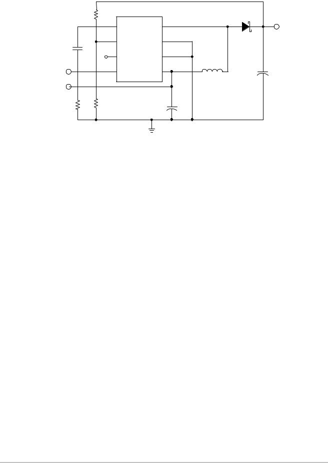
|
R2 |
|
|
3.72 k |
|
|
1 |
VC |
|
|
|
|
2 |
FB |
|
|
|
C1 |
|
|
0.01 F |
3 |
Test |
|
|
|
SS |
4 |
SS |
|
3.3 V 
CS5171/3
|
|
|
D1 |
VOUT |
VSW |
8 |
|
|
|
|
|
5 V |
||
|
|
|
||
PGND |
7 |
|
MBRS120T3 |
|
|
|
|
||
|
|
|
|
|
AGND |
6 |
|
|
|
|
|
|
|
|
|
L1 |
|
|
+ C3 |
VCC |
5 |
|
|
|
22 |
H |
|
22 F |
|
|
|
|||
|
|
|
R1 |
R3 |
+ |
5 k |
1.28 k |
C2 |
|
|
22 F |
Figure 1. Applications Diagram
MAXIMUM RATINGS
Rating |
Value |
Unit |
|
|
|
Junction Temperature Range, TJ |
−40 to +150 |
°C |
|
|
|
Storage Temperature Range, TSTORAGE |
−65 to +150 |
°C |
|
|
|
Package Thermal Resistance: Junction−to−Case, R JC |
45 |
°C/W |
Junction−to−Ambient, R JA |
165 |
°C/W |
Lead Temperature Soldering: Reflow (Note 1) |
230 Peak |
°C |
|
|
|
ESD, Human Body Model |
1.2 |
kV |
|
|
|
Maximum ratings are those values beyond which device damage can occur. Maximum ratings applied to the device are individual stress limit values (not normal operating conditions) and are not valid simultaneously. If these limits are exceeded, device functional operation is not implied, damage may occur and reliability may be affected.
1. 60 second maximum above 183°C.
MAXIMUM RATINGS
Pin Name |
Pin Symbol |
VMAX |
VMIN |
ISOURCE |
ISINK |
IC Power Input |
VCC |
30 V |
−0.3 V |
N/A |
200 mA |
Shutdown/Sync |
SS |
30 V |
−0.3 V |
1.0 mA |
1.0 mA |
|
|
|
|
|
|
Loop Compensation |
VC |
6.0 V |
−0.3 V |
10 mA |
10 mA |
Voltage Feedback Input |
FB |
10 V |
−0.3 V |
1.0 mA |
1.0 mA |
|
(CS5171/3 only) |
|
|
|
|
|
|
|
|
|
|
Negative Feedback Input |
NFB |
−10 V |
10 V |
1.0 mA |
1.0 mA |
(transient, 10 ms) |
(CS5172/4 only) |
|
|
|
|
|
|
|
|
|
|
|
|
|
|
|
|
Test Pin |
Test |
6.0 V |
−0.3 V |
1.0 mA |
1.0 mA |
|
|
|
|
|
|
Power Ground |
PGND |
0.3 V |
−0.3 V |
4 A |
10 mA |
|
|
|
|
|
|
Analog Ground |
AGND |
0 V |
0 V |
N/A |
10 mA |
|
|
|
|
|
|
Switch Input |
VSW |
40 V |
−0.3 V |
10 mA |
3.0 A |
http://onsemi.com
2

CS5171, CS5172, CS5173, CS5174
ELECTRICAL CHARACTERISTICS (2.7 V< VCC < 30 V; Industrial Grade: −40 °C < TJ < 125°C;
Commercial Grade: 0°C < TJ < 125°C; For all CS5171/2/3/4 specifications unless otherwise stated.)
Characteristic |
Test Conditions |
Min |
Typ |
Max |
Unit |
|
|
|
|
|
|
Positive and Negative Error Amplifiers |
|
|
|
|
|
|
|
|
|
|
|
FB Reference Voltage (CS5171/3 only) |
VC tied to FB; measure at FB |
1.246 |
1.276 |
1.300 |
V |
NFB Reference Voltage (CS5172/4 only) |
VC = 1.25 V |
−2.55 |
−2.45 |
−2.35 |
V |
FB Input Current (CS5171/3 only) |
FB = VREF |
−1.0 |
0.1 |
1.0 |
A |
NFB Input Current (CS5172/4 only) |
NFB = NVREF |
−16 |
−10 |
−5.0 |
A |
FB Reference Voltage Line Regulation |
VC = FB |
− |
0.01 |
0.03 |
%/V |
(CS5171/3 only) |
|
|
|
|
|
|
|
|
|
|
|
NFB Reference Voltage Line Regulation |
VC = 1.25 V |
− |
0.01 |
0.05 |
%/V |
(CS5172/4 only) |
|
|
|
|
|
|
|
|
|
|
|
Positive Error Amp Transconductance |
IVC = ± 25 A |
300 |
550 |
800 |
Mho |
Negative Error Amp Transconductance |
IVC = ± 5 A |
115 |
160 |
225 |
Mho |
Positive Error Amp Gain |
(Note 2) |
200 |
500 |
− |
V/V |
|
|
|
|
|
|
Negative Error Amp Gain |
(Note 2) |
100 |
180 |
320 |
V/V |
|
|
|
|
|
|
VC Source Current |
FB = 1.0 V or NFB = −1.9 V, V C = 1.25 V |
25 |
50 |
90 |
A |
VC Sink Current |
FB = 1.5 V or NFB = −3.1 V, V C = 1.25 V |
200 |
625 |
1500 |
A |
VC High Clamp Voltage |
FB = 1.0 V or NFB = −1.9 V; |
1.5 |
1.7 |
1.9 |
V |
|
VC sources 25 A |
|
|
|
|
VC Low Clamp Voltage |
FB = 1.5 V or NFB = −3.1 V, V C sinks 25 A |
0.25 |
0.50 |
0.65 |
V |
VC Threshold |
Reduce VC from 1.5 V until switching stops |
0.75 |
1.05 |
1.30 |
V |
Oscillator |
|
|
|
|
|
|
|
|
|
|
|
Base Operating Frequency |
CS5171/2, FB = 1 V or NFB = −1.9 V |
230 |
280 |
310 |
kHz |
|
|
|
|
|
|
Reduced Operating Frequency |
CS5171/2, FB = 0 V or NFB = 0 V |
30 |
52 |
120 |
kHz |
|
|
|
|
|
|
Maximum Duty Cycle |
CS5171/2 |
90 |
94 |
− |
% |
|
|
|
|
|
|
Base Operating Frequency |
CS5173/4, FB = 1 V or NFB = −1.9 V |
460 |
560 |
620 |
kHz |
|
|
|
|
|
|
Reduced Operating Frequency |
CS5173/4, FB = 0 V or NFB = 0 V |
60 |
104 |
160 |
kHz |
|
|
|
|
|
|
Maximum Duty Cycle |
CS5173/4 |
82 |
90 |
− |
% |
|
|
|
|
|
|
NFB Frequency Shift Threshold |
Frequency drops to reduced operating frequency |
−0.80 |
−0.65 |
−0.50 |
V |
|
|
|
|
|
|
FB Frequency Shift Threshold |
Frequency drops to reduced operating frequency |
0.36 |
0.40 |
0.44 |
V |
|
|
|
|
|
|
Sync/ Shutdown |
|
|
|
|
|
|
|
|
|
|
|
Sync Range |
CS5171/2 |
320 |
− |
500 |
kHz |
|
|
|
|
|
|
Sync Range |
CS5173/4 |
640 |
− |
1000 |
kHz |
|
|
|
|
|
|
Sync Pulse Transition Threshold |
Rise time = 20 ns |
2.5 |
− |
− |
V |
|
|
|
|
|
|
SS Bias Current |
SS = 0 V |
−15 |
−3.0 |
− |
A |
|
SS = 3.0 V |
− |
3.0 |
8.0 |
A |
|
|
|
|
|
|
Shutdown Threshold |
− |
0.50 |
0.85 |
1.20 |
V |
|
|
|
|
|
|
Shutdown Delay |
2.7 V ≤ VCC ≤ 12 V |
12 |
80 |
350 |
s |
|
12 V < VCC ≤ 30 V |
12 |
36 |
200 |
s |
2. Guaranteed by design, not 100% tested in production.
http://onsemi.com
3

CS5171, CS5172, CS5173, CS5174
ELECTRICAL CHARACTERISTICS (continued) (2.7 V< VCC < 30 V; Industrial Grade: −40 °C < TJ < 125°C; Commercial Grade: 0°C < TJ < 125°C; For all CS5171/2/3/4 specifications unless otherwise stated.)
Characteristic |
Test Conditions |
Min |
Typ |
Max |
Unit |
|
|
|
|
|
|
Power Switch |
|
|
|
|
|
|
|
|
|
|
|
Switch Saturation Voltage |
ISWITCH = 1.5 A, (Note 3) |
− |
0.8 |
1.4 |
V |
|
ISWITCH = 1.0 A, 0°C ≤ TJ ≤ 85°C |
− |
0.55 |
− |
V |
|
ISWITCH = 1.0 A, −40 °C ≤ TJ ≤ 0°C |
− |
0.75 |
− |
V |
|
ISWITCH = 10 mA |
− |
0.09 |
0.45 |
V |
Switch Current Limit |
50% duty cycle, Note 3 |
1.6 |
1.9 |
2.4 |
A |
|
80% duty cycle, Note 3 |
1.5 |
1.7 |
2.2 |
A |
|
|
|
|
|
|
Minimum Pulse Width |
FB = 0 V or NFB = 0 V, ISW = 4.0 A, (Note 3) |
200 |
250 |
300 |
ns |
ICC/ IVSW |
2.7 V ≤ VCC ≤ 12 V, 10 mA ≤ ISW ≤ 1.0 A |
− |
10 |
30 |
mA/A |
|
12 V < VCC ≤ 30 V, 10 mA ≤ ISW ≤ 1.0 A |
− |
− |
100 |
mA/A |
|
2.7 V ≤ VCC ≤ 12 V, 10 mA ≤ ISW ≤ 1.5 A, (Note 3) |
− |
17 |
30 |
mA/A |
|
12 V < VCC ≤ 30 V, 10 mA ≤ ISW ≤ 1.5 A, (Note 3) |
− |
− |
100 |
mA/A |
|
|
|
|
|
|
Switch Leakage |
VSW = 40 V, VCC = 0V |
− |
2.0 |
100 |
A |
General |
|
|
|
|
|
|
|
|
|
|
|
Operating Current |
ISW = 0 |
− |
5.5 |
8.0 |
mA |
Shutdown Mode Current |
VC < 0.8 V, SS = 0 V, 2.7 V ≤ VCC ≤ 12 V |
− |
12 |
60 |
A |
|
VC < 0.8 V, SS = 0 V, 12 V ≤ VCC ≤ 30 V |
− |
− |
100 |
|
Minimum Operation Input Voltage |
VSW switching, maximum ISW = 10 mA |
− |
2.45 |
2.70 |
V |
Thermal Shutdown |
(Note 3) |
150 |
180 |
210 |
°C |
|
|
|
|
|
|
Thermal Hysteresis |
(Note 3) |
− |
25 |
− |
°C |
|
|
|
|
|
|
3. Guaranteed by design, not 100% tested in production.
PACKAGE PIN DESCRIPTION
Package |
Pin |
|
Pin # |
Symbol |
Function |
|
|
|
1 |
VC |
Loop compensation pin. The VC pin is the output of the error amplifier and is used for loop compensation, |
|
|
current limit and soft start. Loop compensation can be implemented by a simple RC network as shown in the |
|
|
application diagram on page 2 as R1 and C1. |
|
|
|
2 |
FB |
Positive regulator feedback pin. This pin senses a positive output voltage and is referenced to 1.276 V. When |
(CS5171/3 |
|
the voltage at this pin falls below 0.4 V, chip switching frequency reduces to 20% of the nominal frequency. |
only) |
|
|
|
|
|
2 |
Test |
These pins are connected to internal test logic and should either be left floating or tied to ground. Connection |
(CS5172/4) |
|
to a voltage between 2 V and 6 V shuts down the internal oscillator and leaves the power switch running. |
3 |
|
|
(CS5171/3) |
|
|
|
|
|
3 |
NFB |
Negative feedback pin. This pin senses a negative output voltage and is referenced to −2.5 V. When the volt- |
(CS5172/4) |
|
age at this pin goes above −0.65 V, chip switching frequency reduces to 20% of the nominal frequency. |
|
|
|
4 |
SS |
Synchronization and shutdown pin. This pin may be used to synchronize the part to nearly twice the base |
|
|
frequency. A TTL low will shut the part down and put it into low current mode. If synchronization is not used, |
|
|
this pin should be either tied high or left floating for normal operation. |
|
|
|
5 |
VCC |
Input power supply pin. This pin supplies power to the part and should have a bypass capacitor connected to |
|
|
AGND. |
|
|
|
6 |
AGND |
Analog ground. This pin provides a clean ground for the controller circuitry and should not be in the path of |
|
|
large currents. The output voltage sensing resistors should be connected to this ground pin. This pin is con- |
|
|
nected to the IC substrate. |
|
|
|
7 |
PGND |
Power ground. This pin is the ground connection for the emitter of the power switching transistor. Connection |
|
|
to a good ground plane is essential. |
|
|
|
8 |
VSW |
High current switch pin. This pin connects internally to the collector of the power switch. The open voltage |
|
|
across the power switch can be as high as 40 V. To minimize radiation, use a trace as short as practical. |
|
|
|
http://onsemi.com
4
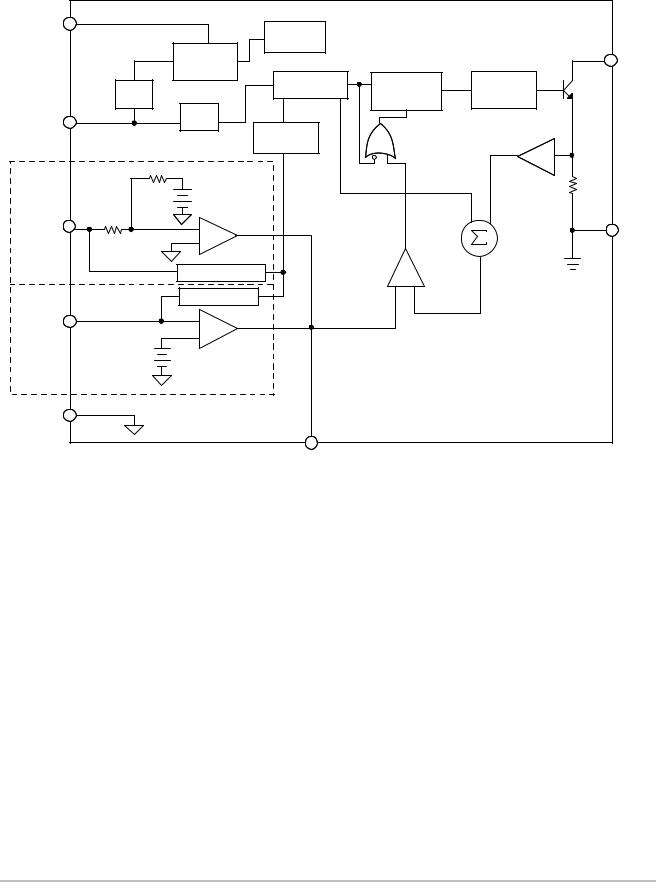
|
|
CS5171, CS5172, CS5173, CS5174 |
|
|
||||
VCC |
|
Thermal |
|
|
|
|
|
|
|
|
Shutdown |
|
|
|
|
|
|
|
Shutdown |
2.0 V |
|
|
|
|
|
VSW |
|
|
Regulator |
|
|
|
|
|
|
|
Delay |
Oscillator |
S |
PWM |
Q |
Driver |
Switch |
|
|
Latch |
|||||||
|
Timer |
|
|
|
R |
|
|
|
|
|
|
|
|
|
|
|
|
SS |
|
Sync |
|
|
|
|
|
|
|
Frequency |
|
|
|
|
|
|
|
|
|
|
|
|
|
|
|
|
|
|
Shift 5:1 |
|
|
|
|
|
|
|
|
|
|
|
|
|
×5 |
|
|
200 k |
|
|
|
Slope |
|
|
|
|
|
Negative |
|
|
Compensation |
|
|
|
|
2.0 V |
|
|
|
|
|
|
|
|
Error Amp |
|
|
|
|
|
63 m |
|
NFB |
250 k |
+ |
|
|
|
|
|
|
|
|
|
|
|
Ramp |
PGND |
||
CS5172/4 |
|
|
|
|
|
|
||
|
− |
|
|
|
|
Summer |
|
|
only |
|
|
|
|
|
|
|
|
|
|
|
|
|
PWM |
|
|
|
|
|
|
|
|
|
|
|
|
|
|
−0.65 V Detector |
|
+ |
|
Comparator |
|
|
|
|
|
− |
|
|
|
||
|
|
|
|
|
|
|
||
|
|
0.4 V Detector |
|
|
|
|
|
|
FB |
|
− |
|
|
|
|
|
|
CS5171/3 |
|
+ |
|
|
|
|
|
|
only |
|
Positive |
|
|
|
|
|
|
|
1.276 V |
Error Amp |
|
|
|
|
|
|
AGND |
|
|
|
|
|
|
|
|
|
|
VC |
|
|
|
|
|
|
Figure 2. Block Diagram
http://onsemi.com
5

CS5171, CS5172, CS5173, CS5174
TYPICAL PERFORMANCE CHARACTERISTICS
|
7.2 |
|
|
|
7.0 |
|
VCC = 30 V |
|
6.8 |
|
|
|
|
|
|
(mA) |
6.6 |
|
|
6.4 |
|
VCC = 12 V |
|
Current |
6.2 |
|
|
6.0 |
|
|
|
|
5.8 |
|
VCC = 2.7 V |
|
5.6 |
50 |
100 |
|
0 |
Temperature (°C)
Figure 3. ICC (No Switching) vs. Temperature
|
70 |
|
|
|
|
60 |
|
|
VCC = 30 V |
(mA/A) |
50 |
ISW = 1.5 A |
|
|
40 |
|
|
|
|
30 |
|
|
VCC = 12 V |
|
|
|
|
||
|
|
|
|
|
|
20 |
|
|
|
|
10 |
|
|
VCC = 2.7 V |
|
0 |
0 |
50 |
100 |
|
|
|||
|
|
|
Temperature (°C) |
|
Figure 4. ICC/ IVSW vs. Temperature
1200 |
|
|
|
|
1.9 |
|
|
|
1000 |
|
|
−40 °C |
|
|
|
|
|
(mV) |
800 |
|
|
85 °C |
|
1.8 |
|
|
|
|
|
|
|
|
|
|
|
CE(SAT) |
600 |
|
|
|
(V) |
1.7 |
|
|
|
|
25 °C |
IN |
|
|
|||
|
|
|
|
|
|
|||
|
|
|
|
V |
|
|
|
|
V |
400 |
|
|
|
1.6 |
|
|
|
|
200 |
|
|
|
|
|
|
|
|
|
|
|
|
|
|
|
|
|
0 |
500 |
1000 |
|
|
1.5 |
50 |
100 |
|
|
|
|
0 |
||||
|
|
|
ISW (mA) |
|
|
|
° |
|
|
|
|
|
|
|
|
Temperature ( C) |
|
Figure 5. VCE(SAT) vs. ISW |
Figure 6. Minimum Input Voltage vs. Temperature |
|
285 |
|
|
280 |
|
(kHz) |
275 |
|
270 |
||
OSC |
||
265 |
||
f |
||
|
260 |
|
|
255 |
0 |
50 |
100 |
|
Temperature (°C) |
|
Figure 7. Switching Frequency vs. Temperature (CS5171/2 only)
fOSC (kHz)
570
565
560
555
550
545
540
535
530
525
520
0 |
50 |
100 |
Temperature (°C)
Figure 8. Switching Frequency vs. Temperature (CS5173/4 only)
http://onsemi.com
6

CS5171, CS5172, CS5173, CS5174
TYPICAL PERFORMANCE CHARACTERISTICS
100
Typical)of |
75 |
|
|
(% |
50 |
|
|
OSC |
25 |
f |
|
|
0 |
VCC = (12 V)
−40 °C
85°C
25°C
350 |
380 |
400 |
420 |
450 |
|
|
VFB (mV) |
|
|
Figure 9. Switching Frequency vs. VFB (CS5171/3 only)
Typical)of |
100 |
|
75 |
||
|
||
(% |
50 |
|
|
||
OSC |
25 |
|
f |
||
|
0 |
VCC = (12 V)
85°C
−40 °C
25°C 
−550 |
−660 |
−725 |
|
VNFB (mV) |
|
Figure 10. Switching Frequency vs. VNFB (CS5172/4 only)
|
1.280 |
|
|
|
|
|
|
|
|
|
1.278 |
|
VCC = 12 V |
|
−2.42 |
|
|
|
|
|
|
|
|
|
|
|
VCC = 30 V |
||
Voltage(V) |
1.276 |
|
|
Voltage(V) |
−2.43 |
|
|
|
|
|
VCC = 30 V |
|
|
|
|
|
|||
1.272 |
|
−2.44 |
|
|
|
|
|||
|
1.274 |
|
|
|
−2.45 |
|
|
|
|
|
|
VCC = 2.7 V |
|
|
V |
CC |
= 12 V |
|
|
|
|
|
|
|
|
|
|
|
|
|
|
|
|
|
−2.46 |
|
|
|
|
|
1.270 |
|
|
|
−2.47 |
|
|
|
|
|
|
|
|
|
|
|
|
VCC = 2.7 V |
|
|
1.268 |
|
|
|
−2.48 |
|
|
|
|
|
50 |
100 |
|
0 |
|
50 |
100 |
||
|
0 |
|
|
|
|||||
|
|
° |
|
|
|
|
|
Temperature (°C) |
|
|
|
Temperature ( C) |
|
|
|
|
|
|
|
Figure 11. Reference Voltage vs. Temperature |
Figure 12. Reference Voltage vs. Temperature |
(CS5171/3 only) |
(CS5172/4 only) |
|
0.20 |
|
|
|
|
|
|
|
|
|
|
|
|
|
|
|
0.18 |
|
|
|
|
|
|
|
|
|
|
|
|
|
|
( A) |
0.16 |
|
|
|
|
|
|
|
|
|
|
VCC = 12 V |
|
||
0.14 |
|
|
|
|
|
||
FB |
|
|
|
|
|
|
|
|
|
|
|
|
|
|
|
I |
0.12 |
|
|
|
|
|
|
|
|
|
|
|
|
|
|
|
|
|
|
|
|
|
|
|
0.10 |
|
|
|
|
|
|
|
|
|
|
|
VCC = 2.7 V |
|
|
|
|
|
|
|
|
|
|
|
0.08 |
|
|
|
|
|
|
|
0 |
50 |
100 |
||||
|
|
||||||
Temperature (°C)
Figure 13. IFB vs. Temperature (CS5171/3 only)
|
−7 |
|
−8 |
( A) |
−9 |
−10 |
|
NFB−11 |
|
I |
|
|
−12 |
−13
−14
0 |
50 |
100 |
|
Temperature (°C) |
|
Figure 14. INFB vs. Temperature (CS5172/ 4 only)
http://onsemi.com
7
 Loading...