


BC337
查询BC337-16RL1供应商
BC337, BC337−16,
BC337−25, BC337−40,
BC338−25
Amplifier Transistors
NPN Silicon
http://onsemi.com
Features
• Pb−Free Package is Available*
MAXIMUM RATINGS
Rating Symbol BC337 BC338 Unit
Collector−Emitter Voltage V
Collector−Base Voltage V
Emitter−Base Voltage V
Collector Current − Continuous I
Total Device Dissipation
@ TA = 25°C
Derate above 25°C
Total Device Dissipation
@ TC = 25°C
Derate above 25°C
Operating and Storage Junction
Temperature Range
CEO
CBO
EBO
P
P
TJ, T
C
D
D
THERMAL CHARACTERISTICS
Characteristic Symbol Max Unit
Thermal Resistance,
Junction−to−Ambient
Thermal Resistance,
Junction−to−Case
Maximum ratings are those values beyond which device damage can occur.
Maximum ratings applied to the device are individual stress limit values (not
normal operating conditions) and are not valid simultaneously. If these limits
are exceeded, device functional operation is not implied, damage may occur
and reliability may be affected.
R
JA
R
JC
45 25 Vdc
50 30 Vdc
5.0 Vdc
800 mAdc
625
5.0
1.5
−55 to +150 °C
stg
200 °C/W
83.3 °C/W
mW
mW/°C
W
mW/°C
12
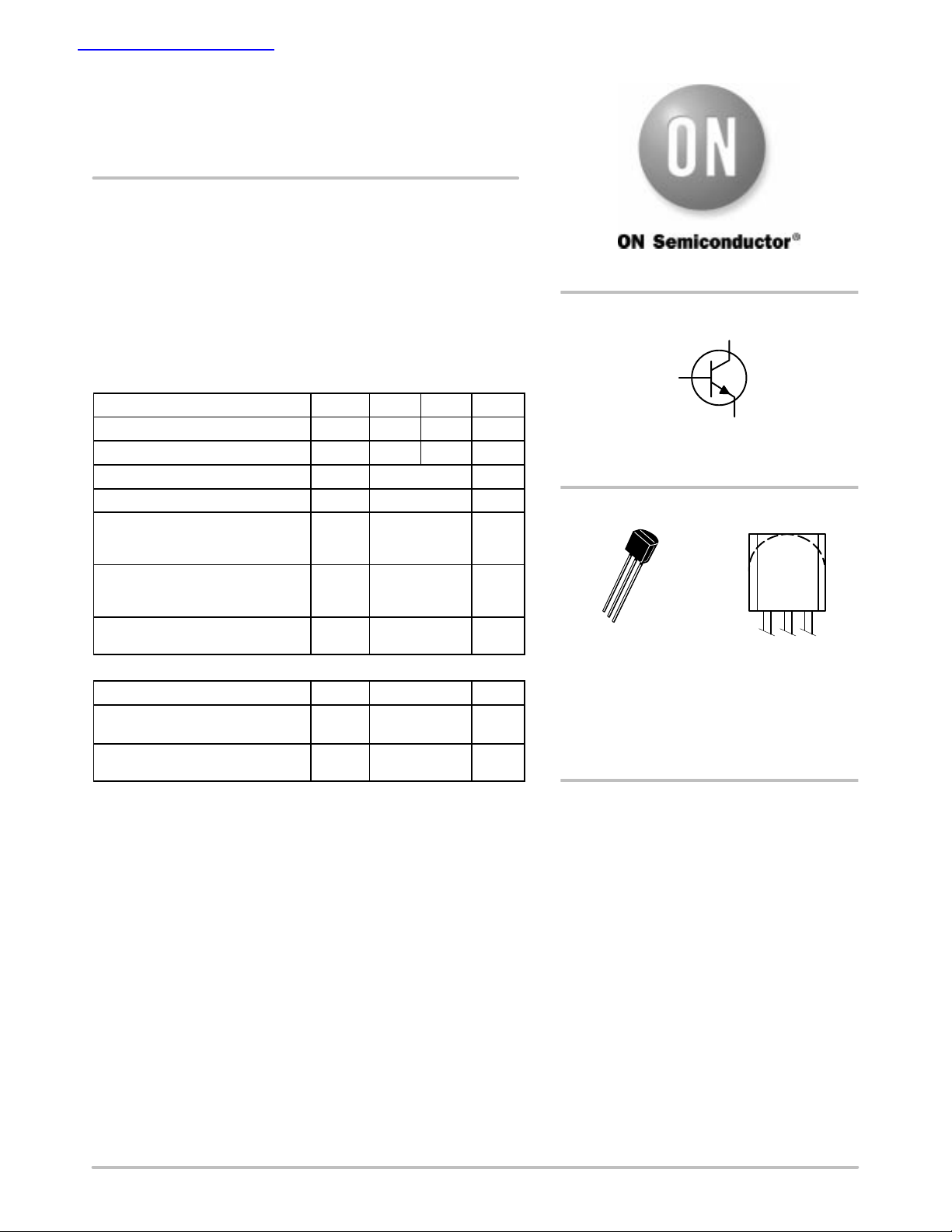
COLLECTOR
1
2
BASE
3
EMITTER
MARKING
DIAGRAM
BC33
xxxx
YWW
TO−92 (TO−226)
CASE 29
xxxx = Specific Device Code
Y = Year
WW = Work Week
ORDERING INFORMATION
See detailed ordering and shipping information in the package
dimensions section on page 4 of this data sheet.
*For additional information on our Pb−Free strategy and soldering details, please
download the ON Semiconductor Soldering and Mounting Techniques
Reference Manual, SOLDERRM/D.
Semiconductor Components Industries, LLC, 2004
July, 2004 − Rev. 4
1 Publication Order Number:
BC337/D
BC337, BC337−16, BC337−25, BC337−40, BC338−25
ELECTRICAL CHARACTERISTICS (T
= 25°C unless otherwise noted)
A
Characteristic
OFF CHARACTERISTICS
Collector−Emitter Breakdown Voltage
(IC = 10 mA, IB = 0) BC337
BC338
Collector−Emitter Breakdown Voltage
(IC = 100 A, IE = 0) BC337
BC338
Emitter−Base Breakdown Voltage
(I
= 10 A, IC = 0)
E
Collector Cutoff Current
(VCB = 30 V, IE = 0) BC337
(V
= 20 V, IE = 0) BC338
CB
Collector Cutoff Current
(VCE = 45 V, VBE = 0) BC337
(V
= 25 V, VBE = 0) BC338
CE
Emitter Cutoff Current
(VEB = 4.0 V, IC = 0)
ON CHARACTERISTICS
DC Current Gain
(IC = 100 mA, VCE = 1.0 V) BC337
BC337−16
BC337−25/BC338−25
BC337−40
(I
= 300 mA, VCE = 1.0 V)
C
Base−Emitter On Voltage
(I
= 300 mA, VCE = 1.0 V)
C
Collector−Emitter Saturation Voltage
(IC = 500 mA, IB = 50 mA)
SMALL−SIGNAL CHARACTERISTICS
Output Capacitance
(VCB = 10 V, IE = 0, f = 1.0 MHz)
Current−Gain − Bandwidth Product
(IC = 10 mA, VCE = 5.0 V, f = 100 MHz)
Symbol Min Typ Max Unit
V
(BR)CE
V
(BR)CE
V
(BR)EB
I
CBO
I
CES
I
EBO
h
V
BE(on)
V
CE(sat)
C
O
S
O
FE
f
45
25
50
30
−
−
−
−
−
−
−
−
5.0 − − Vdc
−
−
−
−
−
−
−
−
100
100
100
100
− − 100 nAdc
100
100
160
250
60
−
−
−
−
−
630
250
400
630
−
− − 1.2 Vdc
− − 0.7 Vdc
ob
T
− 15 − pF
− 210 − MHz
Vdc
Vdc
nAdc
nAdc
−
1.0
0.7
0.5
0.3
0.2
0.1
0.07
0.05
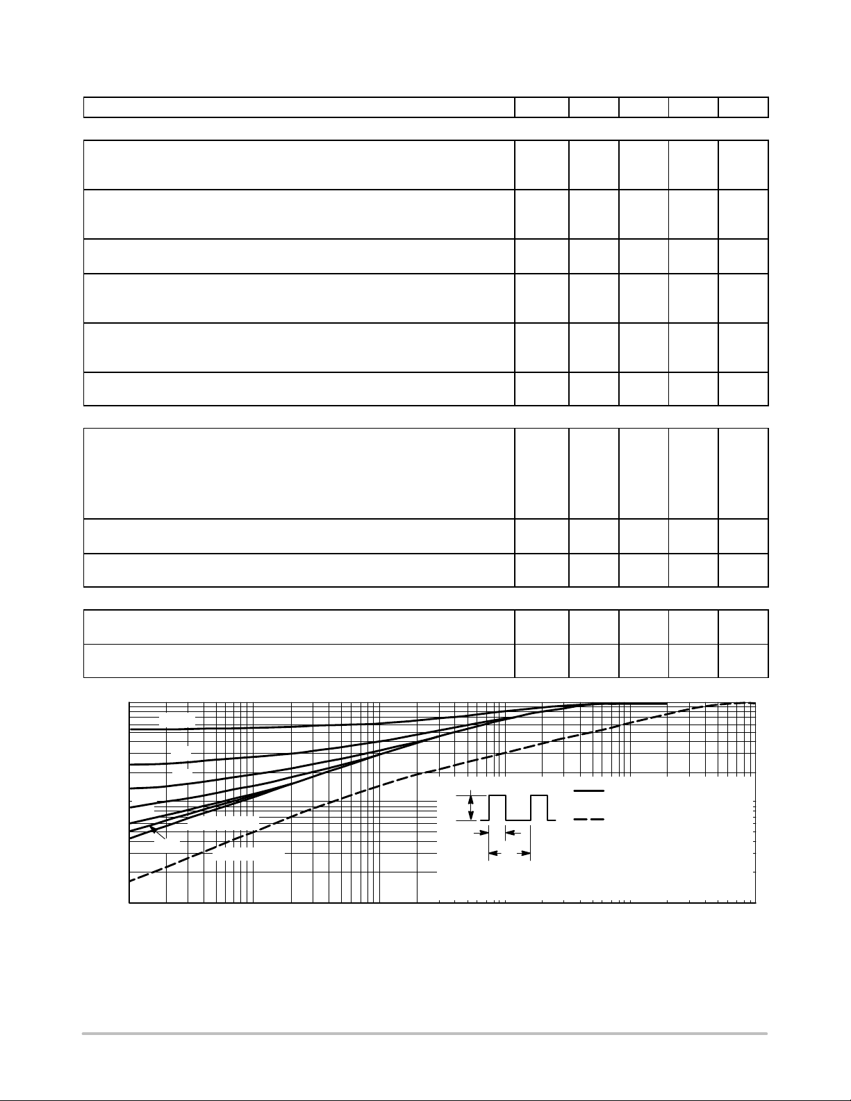
THERMAL RESISTANCE
0.03
0.02
r(t), NORMALIZED EFFECTIVE TRANSIENT
0.01
D = 0.5
0.2
0.05
0.02
0.1
0.01
SINGLE PULSE
SINGLE PULSE
P
(pk)
t
1
t
2
DUTY CYCLE, D = t1/t
2
(t) = (t)
JC
JC
JA
JA
JC
= 100°C/W MAX
(t) = r(t)
JA
= 375°C/W MAX
D CURVES APPLY FOR
POWER
PULSE TRAIN SHOWN
READ TIME AT t
T
− TC = P
J(pk)
(pk) JC
0.001 0.002 0.005 0.01 0.02 0.05 0.1 0.2 0.5 1.0 2.0 5.0 10 20 50 100
t, TIME (SECONDS)
Figure 1. Thermal Response
http://onsemi.com
2
1
(t)
 Loading...