


NCP1397A,"NCP1397-D" NCP1397B
High Performance Resonant Mode Controller with Integrated High--Voltage Drivers
The NCP1397 is a high performance controller that can be utilized in half bridge resonant topologies such as series resonant, parallel resonant and LLC resonant converters. It integrates 600 V gate drivers, simplifying layout and reducing external component count. With its unique architecture, including a 500 kHz Voltage Controlled Oscillator whose control mode permits flexibility when an ORing function is required, the NCP1397 delivers everything needed to build a reliable and rugged resonant mode power supply.
The NCP1397 provides a suite of protection features with configurable settings to optimize any application. These include: auto-recovery or fault latch-off, brown-out, open optocoupler, soft-start and short-circuit protection. Deadtime is also adjustable to overcome shoot through current.
Features
High-Frequency Operation from 50 kHz up to 500 kHz
600 V High-Voltage Floating Driver
Adjustable Minimum Switching Frequency with ±3% Accuracy
Adjustable Deadtime from 100 ns to 2 ms.
Startup Sequence Via an Externally Adjustable Soft-Start
Brown-Out Protection for a Simpler PFC Association
Latched Input for Severe Fault Conditions, e.g. Over Temperature or OVP
Timer-Based Input with Auto-Recovery Operation for Delayed Event Reaction
Latched Overcurrent Protection
Disable Input for Immediate Event Reaction or Simple ON/OFF Control
VCC Operation up to 20 V
Low Startup Current of 300 mA
1 A / 0.5 A Peak Current Sink / Source Drive Capability
Common Collector Optocoupler Connection for Easier ORing
Optional Common Emitter Optocoupler Connection
Internal Temperature Shutdown
These Devices are Pb-Free, Halogen Free/BFR Free and are RoHS Compliant
Typical Applications
|
http://onsemi.com |
|
|||
|
|
|
MARKING |
||
|
|
|
DIAGRAMS |
||
16 |
|
16 |
|
|
|
1 |
|
|
NCP1397xG |
||
|
|
AWLYWW |
|||
SO-16, LESS PIN 13 |
|||||
|
|
||||
D SUFFIX |
1 |
|
|
||
CASE 751AM |
|
|
|
||
x |
|
= A or B |
|
|
|
A |
|
= Assembly Location |
|||
WL |
|
= Wafer Lot |
|
|
|
Y |
|
= Year |
|
|
|
WW |
= Work Week |
|
|||
G |
|
= Pb--Free Package |
|||
|
PIN CONNECTIONS |
|
|||
CSS(dis) |
1 |
|
16 |
Vboot |
|
Fmax |
2 |
|
15 |
Mupper |
|
Ctimer |
3 |
|
14 |
HB |
|
Rt |
4 |
|
|
|
|
BO |
5 |
|
12 |
VCC |
|
FB |
6 |
|
11 |
Mlower |
|
DT |
7 |
|
10 |
GND |
|
Skip/Disable |
8 |
|
9 |
Fault |
|
(Top View)
ORDERING INFORMATION
Seedetailedorderingandshippinginformationinthepackage dimensions section on page 26 of this data sheet.
Flat Panel Display Power Converters |
Industrial and Medical Power Sources |
High Power ac-dc Adapters for Notebooks |
Offline Battery Chargers |
Computing Power Supplies |
|
Semiconductor Components Industries, LLC, 2010 |
1 |
Publication Order Number: |
November, 2010 - Rev. 2 |
|
NCP1397/D |
NCP1397A, NCP1397B
"NCP1397-D"
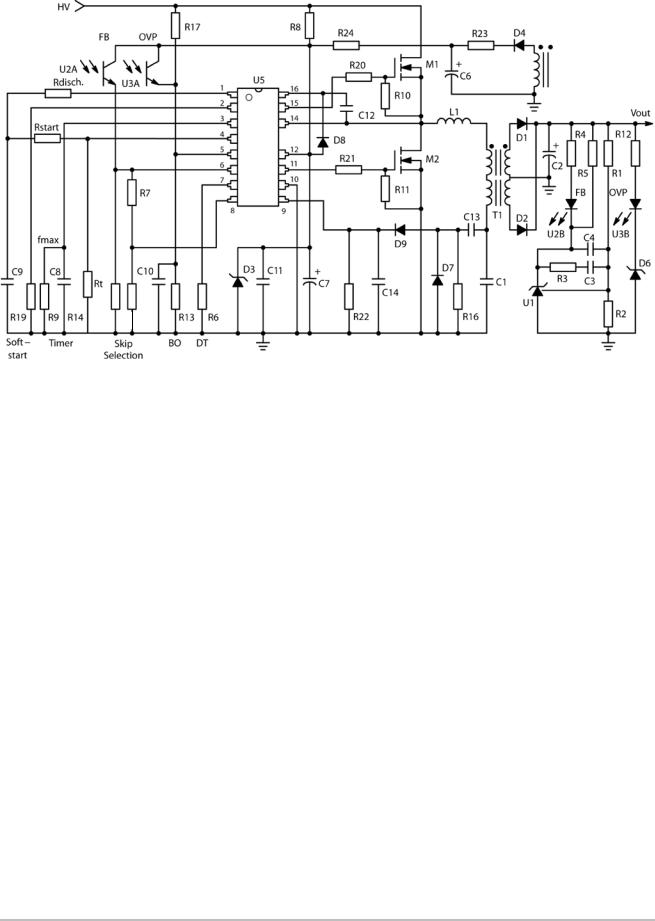
R18
Figure 1. Typical Application Example
PIN FUNCTION DESCRIPTION
Pin # |
Pin Name |
Function |
Pin Description |
|
|
|
|
1 |
CSS(dis) |
Soft--Start Discharge |
Soft--start capacitor discharge pin. Connect to the soft--start capacitor to reset it |
|
|
|
before startup or during overload conditions. |
|
|
|
|
2 |
Fmax |
Maximum frequency clamp |
A resistor sets the maximum frequency excursion |
|
|
|
|
3 |
Ctimer |
Timer duration |
Sets the timer duration in presence of a fault |
|
|
|
|
4 |
Rt |
Minimum frequency clamp |
Connecting a resistor to this pin, sets the minimum oscillator frequency reached |
|
|
|
for VFB = 1 V. |
5 |
BO |
Brown--Out |
Detects low input voltage conditions. When brought above Vlatch (4 V typically), it |
|
|
|
fully latches off the controller. |
|
|
|
|
6 |
FB |
Feedback |
Injecting current into this pin increases the oscillation frequency up to Fmax. |
|
|
|
|
7 |
DT |
Deadtime |
A simple resistor adjusts the dead--time width |
|
|
|
|
8 |
Skip/Disable |
Skip or Disable input |
Upon release, a clean startup sequence occurs if VFB < 0.3 V. During the skip |
|
|
|
mode, when FB doesn’t drop below 0.3 V, the IC restarts without soft--start |
|
|
|
sequence. |
|
|
|
|
9 |
Fault |
Fault detection input |
When asserted, the external timer starts to countdown and shuts down the |
|
|
|
controller at the end of its time duration. Simultaneously the Soft--Start discharge |
|
|
|
switch is activated so the converter operating frequency goes up to protect |
|
|
|
application power stage. This input features also second fault comparator with |
|
|
|
higher threshold (1.5 V typically) that: |
|
|
|
A) Speeds up the timer capacitor charging current 8 times – NCP1397A |
|
|
|
B) latches off the IC permanently – NCP1397B |
|
|
|
In both versions the second fault comparator helps to protect application in case |
|
|
|
of short circuit on the output or transformer secondary winding. |
|
|
|
|
10 |
GND |
Analog ground |
-- |
|
|
|
|
11 |
Mlower |
Low side output |
Drives the lower side MOSFET |
|
|
|
|
12 |
VCC |
Supplies the controller |
The controller accepts up to 20 V |
13 |
NC |
Not connected |
Increases the creepage distance |
|
|
|
|
14 |
HB |
Half--bridge connection |
Connects to the half--bridge output |
|
|
|
|
15 |
Mupper |
High side output |
Drives the higher side MOSFET |
|
|
|
|
16 |
Vboot |
Bootstrap pin |
The floating VCC supply for the upper stage |
http://onsemi.com
2
|
|
|
|
|
NCP1397A, NCP1397B |
|
|
|||
|
|
VDD |
|
|
|
|
|
|
|
|
"NCP1397-D" |
|
|
|
|
|
Temperature |
|
|
||
|
|
|
|
|
|
|
|
Shutdown |
|
|
|
|
Imin |
|
|
|
S |
|
|
|
VBOOT |
|
|
|
|
|
|
|
|
|
||
|
|
VFB VFB(off) |
|
|
D |
|
Q |
|
|
|
|
Vref |
|
|
+ |
|
Clk |
Q |
Vref |
|
|
|
|
|
|
|
|
|
|
|||
|
|
|
|
-- |
|
|
|
|
||
|
|
|
|
|
|
|
|
|
|
|
Rt |
|
|
+ |
|
R |
|
|
|
|
|
|
|
IDT |
|
|
|
|
|
|||
|
C |
|
|
|
FF |
|
|
|||
|
|
|
|
|
|
|
|
|||
|
|
|
|
|
|
|
|
|
||
|
|
|
|
DT Adj. |
|
50% DC |
VCC Management |
|
Mupper |
|
|
|
|
|
|
|
|
||||
I = Imax for Vfb = 5.3 V |
|
|
|
|
|
|
|
|
|
|
I = 0 for Vfb < Vfb(min) |
|
|
|
|
|
|
BO |
|
|
|
|
|
|
|
|
|
|
|
|
|
|
|
|
VDD |
|
|
|
|
|
Reset |
|
|
|
|
|
|
|
|
|
|
|
|
|
|
|
|
|
|
|
|
|
PON |
|
|
|
|
Imax |
|
|
|
|
|
Reset |
|
UVLO |
|
|
|
|
|
|
|
|
|
||
|
|
VFB = 5 |
|
|
|
|
|
Fault |
|
|
|
VDD |
Vdd |
|
|
|
|
|
Timeout |
Fast |
|
|
|
|
|
|
|
|
|
Fault |
|
|
|
|
|
|
|
|
|
|
Fault |
HB |
|
|
Vref |
|
|
|
|
|
|
|
||
|
|
|
|
|
|
|
|
|
||
|
|
|
|
|
|
|
|
|
|
|
|
Itimer1 |
Itimer2 |
|
|
|
|
|
|
|
|
Fmax |
|
|
|
|
|
|
|
|
|
|
Timer |
|
|
|
|
|
|
|
|
Level |
|
|
+ |
|
|
|
|
|
|
Shifter |
NC |
|
|
|
-- |
|
|
Timeout |
|
|
|
|
|
|
|
+ |
|
|
Fault |
|
|
|
|
|
|
|
|
|
|
|
|
|
|
|
|
|
|
Vref |
|
|
|
|
|
|
|
|
|
|
|
|
PON |
|
|
|
|
|
|
|
|
|
|
Reset |
|
|
|
|
|
|
|
|
|
|
Fault |
|
|
|
|
|
VCC |
|
|
|
|
|
|
|
|
|
|
|
|
|
|
|
|
|
|
|
Fault |
|
|
SS(dis) |
|
|
|
|
|
|
|
|
|
|
FB |
|
|
+ |
G = 1 |
|
|
|
|
|
Mlower |
|
|
|
-- |
|
> 0 only |
VDD |
|
|
|
|
|
|
|
|
|
V = V(FB) -- VFB(min) |
|
|
|
|
|
RFB |
+ |
|
|
|
|
|
|
|
|
|
|
-- |
|
|
|
|
|
|
|
|
GND |
|
+ |
|
+ |
|
|
|
|
|
|
|
|
|
|
|
|
|
|
|
|
||
|
VFB(fault) |
|
VFB(min) |
|
|
|
|
|
|
|
|
|
|
|
|
|
|
|
|
||
|
|
|
|
|
|
|
|
|
-- |
Skip/ |
|
|
|
|
|
|
|
|
|
Disable |
|
|
|
|
|
|
|
|
|
|
|
|
|
|
|
|
|
Vref |
|
|
|
+ |
20 ns Noise |
|
|
|
|
|
|
|
|
|
Filter |
|
|
|
|
|
|
|
|
|
|
|
|
|
IDT |
|
|
|
|
Deadtime |
|
Vref Skip/Disable |
+ |
|
DT |
|
|
|
|
Adjustment |
|
|
|||
|
|
|
|
|
|
|
|
|||
|
VDD |
|
|
|
|
|
|
|
|
|
|
IBO |
|
20 ms Noise |
|
|
|
|
|
Filter |
|
|
|
|
|
|
|
|
Q |
Q |
|
BO |
+ |
|
+ |
S |
R |
PON Reset |
|
-- |
|
-- |
|||
|
|
20 ms Noise |
|
|
||
|
+ |
|
+ |
|
|
|
|
VBO |
|
Vlatch |
Filter |
|
|
Fault |
|
+ |
|
|
|
|
|
|
-- |
|
|
|
|
|
+ |
|
+ |
|
|
|
|
Vref(fault) |
|
-- |
|
|
|
|
|
|
1 ms Noise |
|
|
|
|
|
Vref(OCP) |
+ |
|
|
|
|
|
Filter |
|
|
||
|
|
|
|
|
||
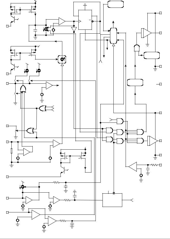
Figure 2. Internal Circuit Architecture (NCP1397A)
http://onsemi.com
3
|
|
|
|
|
NCP1397A, NCP1397B |
|
|
|
||
|
|
VDD |
|
|
|
|
|
|
|
|
"NCP1397-D" |
|
|
|
|
Temperature |
|
|
|||
|
|
|
|
|
|
|
|
|
||
|
|
|
|
|
|
|
|
Shutdown |
|
|
|
|
Imin |
|
|
|
S |
|
|
|
VBOOT |
|
|
VFB VFB(off) |
D |
|
Q |
|
|
|
||
|
Vref |
|
|
+ |
|
Clk |
Q |
Vref |
|
|
|
|
|
|
-- |
|
|
|
|
||
|
|
|
|
|
|
|
|
|
|
|
Rt |
|
|
|
+ |
|
R |
|
|
|
|
|
|
IDT |
|
|
|
|
|
|
||
|
C |
|
|
|
|
FF |
|
|
||
|
|
|
|
|
|
|
|
|||
|
|
|
|
|
|
|
|
|
||
|
|
|
|
DT Adj. |
|
50% DC |
VCC Management |
|
Mupper |
|
|
|
|
|
|
|
|
||||
I = Imax for Vfb = 5.3 V |
|
|
|
|
|
|
|
|
|
|
I = 0 for Vfb < Vfb_min |
|
|
|
|
|
|
BO |
|
|
|
|
|
|
|
|
|
|
|
|
|
|
|
|
VDD |
|
|
|
|
|
Reset |
|
|
|
|
|
|
|
|
|
|
|
|
|
|
|
|
|
|
|
|
PON |
|
|
|
|
|
Imax |
|
|
|
|
Reset |
|
UVLO |
|
|
|
|
|
|
|
|
|
|
||
|
|
Vfb = 5 |
|
|
|
|
Fault |
|
|
|
|
VDD |
|
|
|
|
|
Timeout |
|
Fast |
|
|
|
|
|
|
|
|
|
Fault |
|
|
|
|
|
|
|
|
|
Fault |
|
HB |
|
|
Vref |
|
|
|
|
|
|
|
||
|
|
|
|
|
|
|
|
|
||
|
|
|
|
|
|
|
|
|
|
|
|
Itimer1 |
|
|
|
|
|
|
|
|
|
Fmax |
|
|
|
|
|
|
|
|
|
|
|
If FAULT Itimer else 0 |
|
|
|
|
|
|
|
|
|
|
|
+ |
|
|
|
|
|
|
Level |
|
Timer |
|
|
|
|
|
|
|
Shifter |
NC |
|
|
|
-- |
|
|
|
|
|
|
|
|
|
|
|
|
Timeout |
|
|
|
|
|
|
|
|
|
|
|
Fault |
|
|
|
|
|
|
+ |
|
|
|
|
|
|
|
|
|
|
Vref |
|
|
|
|
|
|
|
|
|
|
|
|
|
PON |
|
|
|
|
|
|
|
|
|
|
Reset |
|
|
|
|
|
|
|
|
|
|
Fault |
|
|
|
|
|
VCC |
|
|
|
|
|
|
|
|
|
|
|
|
|
|
|
|
|
|
Fault |
|
|
|
SS(dis) |
|
|
|
|
|
|
|
|
|
|
FB |
|
|
|
G = 1 |
|
|
|
|
|
Mlower |
|
|
|
+ |
|
|
|
|
|
||
|
|
|
|
|
|
|
|
|
||
|
|
|
|
-- |
> 0 only |
VDD |
|
|
|
|
|
|
|
|
|
V = V(FB) -- VFB(min) |
|
|
|
|
|
RFB |
+ |
|
|
|
|
|
|
|
|
|
|
-- |
|
|
|
|
|
|
|
|
GND |
|
+ |
|
|
+ |
|
|
|
|
|
|
|
|
|
|
|
|
|
|
|
||
|
VFB(fault) |
|
|
VFB(min) |
|
|
|
|
|
|
|
|
|
|
|
|
|
|
|
|
|
|
|
|
|
|
|
|
|
|
-- |
Skip/ |
|
|
|
|
|
|
|
|
|
Disable |
|
|
|
|
|
|
|
|
|
|
|
|
|
|
|
|
|
Vref |
|
|
|
+ |
20 ns Noise |
|
|
|
|
|
|
|
|
|
Filter |
|
|
|
|
|
|
|
|
|
|
|
|
|
IDT |
|
|
|
|
Deadtime |
|
+ |
|
|
DT |
|
|
|
|
Adjustment |
|
Vref Skip |
|
||
|
|
|
|
|
|
|
|
|||
|
VDD |
|
|
|
|
|
|
|
|
|
|
IBO |
|
|
20 ms Noise |
|
|
|
|
|
|
|
|
|
Filter |
|
|
|
|
|
|
|
|
|
|
|
|
|
|
Q |
Q |
|
|
BO |
+ |
|
|
+ |
|
|
|
R |
PON Reset |
|
|
-- |
|
|
-- |
|
|
S |
|
||
|
|
|
20 ms Noise |
|
|
|
|
|||
|
+ |
|
|
+ |
|
|
|
|
|
|
|
VBO |
|
|
Vlatch |
Filter |
|
|
|
|
|
Fault |
+ |
|
|
|
|
|
|
|
|
|
|
-- |
|
|
|
|
|
|
|
|
|
|
+ |
|
+ |
|
|
|
|
|
|
|
|
Vref(fault) |
|
-- |
1 ms Noise |
|
|
|
|
|
|
|
|
|
|
|
|
|
|
|||
|
Vref(OCP) |
+ |
Filter |
|
|
|
|
|
||
|
|
|
|
|
|
|
||||
|
|
|
|
|
|
|
|
|
||
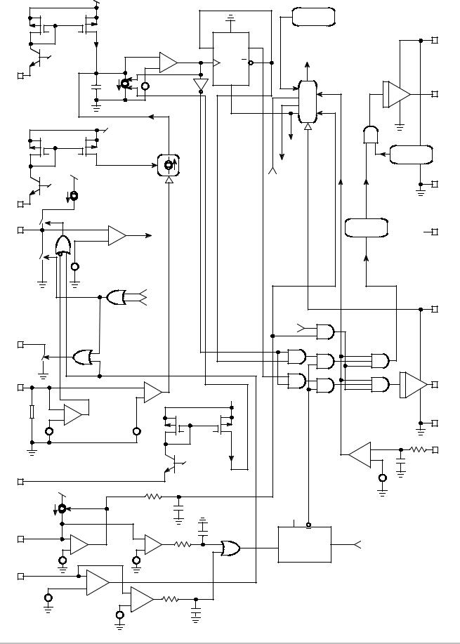
Figure 3. Internal Circuit Architecture (NCP1397B)
http://onsemi.com
4

NCP1397A, NCP1397B
MAXIMUM RATINGS |
|
|
|
|
"NCP1397-D" |
|
|
|
|
|
Rating |
Symbol |
Value |
Unit |
|
|
|
|
|
High Voltage bridge pin, pin 14 |
VBRIDGE |
--1 to 600 |
V |
|
Floating supply voltage, ground referenced |
VBOOT -- VBRIDGE |
0 to 20 |
V |
|
High side output voltage |
VDRV(HI) |
VBRIDGE--0.3 to |
V |
|
|
|
|
VBOOT+0.3 |
|
Low side output voltage |
VDRV(LO) |
--0.3 to VCC+0.3 |
V |
|
Allowable output slew rate |
dVBRIDGE/dt |
50 |
V/ns |
|
Power Supply voltage, pin 12 |
VCC |
20 |
V |
|
Maximum voltage, all pins (except pin 11 and 10) |
-- |
--0.3 to 10 |
V |
|
|
|
|
|
|
Thermal Resistance Junction--to--Air, PDIP version |
RθJA |
100 |
C/W |
|
|
|
|
|
|
Thermal Resistance Junction--to--Air, SOIC version |
RθJA |
130 |
C/W |
|
|
|
|
|
|
Storage Temperature Range |
-- |
--60 to +150 |
C |
|
|
|
|
|
|
ESD Capability, Human Body Model (HBM) (All pins except HV pins) |
-- |
2 |
kV |
|
|
|
|
|
|
ESD Capability, Machine Model (MM) |
-- |
200 |
V |
|
|
|
|
|
|
Stresses exceeding Maximum Ratings may damage the device. Maximum Ratings are stress ratings only. Functional operation above the Recommended Operating Conditions is not implied. Extended exposure to stresses above the Recommended Operating Conditions may affect device reliability.
1.This device(s) contains ESD protection and exceeds the following tests: Human Body Model 2000 V per JEDEC Standard JESD22--A114E Machine Model 200 V per JEDEC Standard JESD22--A115--A
2.This device meets latchup tests defined by JEDEC Standard JESD78.
http://onsemi.com
5

NCP1397A, NCP1397B
ELECTRICAL CHARACTERISTICS (For typical values T |
J |
= 25 C, for min/max values T = --40 C to +125 C, Max T |
J |
= 150 C, V |
CC |
|||||||
"NCP1397-D" |
|
J |
|
|
|
|
|
|||||
= 12 V unless otherwise noted) |
|
|
|
|
|
|
|
|
|
|
|
|
|
|
|
|
|
|
|
|
|
|
|
||
Symbol |
|
Rating |
|
|
Pin |
Min |
Typ |
|
Max |
Unit |
||
|
|
|
|
|
|
|
|
|
|
|
|
|
SUPPLY SECTION |
|
|
|
|
|
|
|
|
|
|
||
|
|
|
|
|
|
|
|
|
|
|
||
VCC(on) |
Turn--on threshold level, VCC going up |
|
|
12 |
9.7 |
10.5 |
|
11.3 |
V |
|||
VCC(min) |
Minimum operating voltage after turn--on |
|
|
12 |
8.7 |
9.5 |
|
10.3 |
V |
|||
Vboot(on) |
Startup voltage on the floating section |
|
|
16--14 |
8 |
9 |
|
|
10 |
V |
||
Vboot(min) |
Cutoff voltage on the floating section |
|
|
16--14 |
7.4 |
8.4 |
|
9.4 |
V |
|||
Istartup |
Startup current, VCC < VCC(on) |
|
|
12 |
-- |
-- |
|
300 |
mA |
|||
VCC(reset) |
VCC level at which the internal logic gets reset |
|
|
12 |
-- |
6.6 |
|
|
-- |
V |
||
ICC1 |
Internal IC consumption, no output load on pin 15/14 – 11/10, |
12 |
-- |
4 |
|
|
-- |
mA |
||||
|
FSW = 300 kHz |
|
|
|
|
|
|
|
|
|
|
|
ICC2 |
Internal IC consumption, 1 nF output load on pin 15/14 – 11/10, |
12 |
-- |
11 |
|
|
-- |
mA |
||||
|
FSW = 300 kHz |
|
|
|
|
|
|
|
|
|
|
|
ICC3 |
Consumption in fault or disable mode (All drivers disabled, |
12 |
-- |
1.5 |
|
|
-- |
mA |
||||
|
Rt = 34 kΩ, RDT = 10 kΩ) |
|
|
|
|
|
|
|
|
|
|
|
VOLTAGE CONTROL OSCILLATOR (VCO) |
|
|
|
|
|
|
|
|
|
|
||
|
|
|
|
|
|
|
|
|
||||
FSW(min) |
Minimum switching frequency, Rt = 34 kΩ on pin 4, Vpin6 = 0.8 V, |
4 |
58.2 |
60 |
|
61.8 |
kHz |
|||||
|
DT = 300 ns |
|
|
|
|
|
|
|
|
|
|
|
|
|
|
|
|
|
|
|
|
||||
FSW(max) |
Maximum switching frequency, Rf(max) = 1.9 kΩ on pin 2, Vpin6 > |
2 |
440 |
500 |
|
560 |
kHz |
|||||
|
5.3 V, Rt = 34 kΩ, DT = 300 ns |
|
|
|
|
|
|
|
|
|
|
|
|
|
|
|
|
|
|
|
|
|
|
|
|
FBSW |
Feedback pin swing above which f = 0 |
|
|
6 |
-- |
5.3 |
|
|
-- |
V |
||
DC |
Operating duty--cycle symmetry |
|
|
11--15 |
48 |
50 |
|
|
52 |
% |
||
|
|
|
|
|
|
|
|
|
|
|||
Tdel1 |
Delay before driver restart from fault or disable mode |
-- |
-- |
700 |
|
|
-- |
ns |
||||
Tdel2 |
Delay before driver restart after VCC(on) event (Note 4) |
-- |
-- |
11 |
|
|
-- |
ms |
||||
Vref(Rt) |
Reference voltage for Rt pin |
|
|
4 |
2.18 |
2.3 |
|
2.42 |
V |
|||
FEEDBACK SECTION |
|
|
|
|
|
|
|
|
|
|
||
|
|
|
|
|
|
|
|
|
|
|
|
|
RFB |
Internal pulldown resistor |
|
|
6 |
-- |
20 |
|
|
-- |
kΩ |
||
VFB(min) |
Voltage on pin 6 below which the FB level has no VCO action |
6 |
-- |
1.1 |
|
|
-- |
V |
||||
VFB(off) |
Voltage on pin 6 below which the controller considers the FB fault |
6 |
240 |
280 |
|
320 |
mV |
|||||
VFBoff(hyste) |
Feedback fault comparator hysteresis |
|
|
6 |
-- |
45 |
|
|
-- |
mV |
||
DRIVE OUTPUT |
|
|
|
|
|
|
|
|
|
|
||
|
|
|
|
|
|
|
|
|
|
|||
Tr |
Output voltage risetime @ CL = 1 nF, 10--90% of output signal |
15--14/11--10 |
-- |
40 |
|
|
-- |
ns |
||||
Tf |
Output voltage falltime @ CL = 1 nF, 10--90% of output signal |
15--14/11--10 |
-- |
20 |
|
|
-- |
ns |
||||
ROH |
Source resistance |
|
|
15--14/11--10 |
-- |
13 |
|
|
-- |
Ω |
||
ROL |
Sink resistance |
|
|
15--14/11--10 |
-- |
5.5 |
|
|
-- |
Ω |
||
Tdead |
Deadtime with RDT = 10 kΩ from pin 7 to GND |
|
|
7 |
250 |
290 |
|
340 |
ns |
|||
Tdead(max) |
Maximum deadtime with RDT = 82 kΩ from pin 7 to GND |
7 |
-- |
2 |
|
|
-- |
ms |
||||
Tdead(min) |
Minimum deadtime, RDT = 3 kΩ from pin 7 to GND |
7 |
-- |
100 |
|
|
-- |
ns |
||||
IHV(LEAK) |
Leakage current on high voltage pins to GND |
|
|
14, 15,16 |
-- |
-- |
|
|
5 |
mA |
||
TIMERS |
|
|
|
|
|
|
|
|
|
|
|
|
|
|
|
|
|
|
|
|
|
||||
Itimer1 |
Timer capacitor charge current during feedback fault or when |
3 |
150 |
175 |
|
190 |
mA |
|||||
|
Vref(fault) < Vpin9 < Vref(OCP) |
|
|
|
|
|
|
|
|
|
|
|
3.The IC does not activate soft--start (unless the feedback pin voltage is below 0.3 V) when the skip/disable input is released, this is for skip cycle implementation.
4.Guaranteed by design.
http://onsemi.com
6

NCP1397A, NCP1397B
ELECTRICAL CHARACTERISTICS (For typical values T |
J |
= 25 C, for min/max values T |
= --40 C to +125 C, Max T |
= 150 C, V |
CC |
|||||||
"NCP1397-D" |
|
J |
|
|
|
|
J |
|
||||
= 12 V unless otherwise noted) |
|
|
|
|
|
|
|
|
|
|
|
|
|
|
|
|
|
|
|
|
|
|
|
||
Symbol |
|
Rating |
|
|
Pin |
|
Min |
Typ |
Max |
Unit |
||
|
|
|
|
|
|
|
|
|
|
|
|
|
TIMERS |
|
|
|
|
|
|
|
|
|
|
|
|
|
|
|
|
|
|
|
|
|
||||
Itimer2 |
Timer capacitor charge current when Vpin9 > Vref(OCP) (Icharge1 + |
3 |
|
1.1 |
1.3 |
|
1.5 |
mA |
||||
|
Icharge2) – A version only |
|
|
|
|
|
|
|
|
|
|
|
Ttimer |
Timer duration with a 1 mF capacitor and a 1 MΩ resistor, Itimer1 |
3 |
|
-- |
24 |
|
-- |
ms |
||||
|
current applied |
|
|
|
|
|
|
|
|
|
|
|
|
|
|
|
|
|
|
|
|
|
|||
TtimerR |
Timer recurrence in permanent fault, same values as above |
3 |
|
-- |
1.4 |
|
-- |
s |
||||
Vtimer(on) |
Voltage at which pin 3 stops output pulses |
|
|
3 |
|
3.8 |
4 |
|
4.2 |
V |
||
Vtimer(off) |
Voltage at which pin 3 restarts output pulses |
|
|
3 |
|
0.95 |
1 |
|
1.05 |
V |
||
RSS(dis) |
Soft--start discharge switch channel resistance |
|
|
1 |
|
-- |
100 |
|
-- |
Ω |
||
PROTECTION |
|
|
|
|
|
|
|
|
|
|
||
|
|
|
|
|
|
|
|
|
|
|||
Vref(Skip) |
Reference voltage for Skip/Disable input (Note 4) |
|
8 |
|
630 |
660 |
|
690 |
mV |
|||
Hyste(Skip) |
Hysteresis for Skip/Disable (Note 4) |
|
|
8 |
|
-- |
45 |
|
-- |
mV |
||
Vref(Fault) |
Reference voltage for Fault comparator |
|
|
9 |
|
0.99 |
1.04 |
|
1.09 |
V |
||
Hyste(Fault) |
Hysteresis for fault comparator input |
|
|
9 |
|
-- |
60 |
|
-- |
mV |
||
Vref(OCP) |
Reference voltage for OCP comparator |
|
|
9 |
|
1.47 |
1.55 |
|
1.63 |
V |
||
Hyste(OCP) |
Hysteresis for OCP comparator input |
|
|
9 |
|
-- |
90 |
|
-- |
mV |
||
Tp(Disable) |
Propagation delay from disable input to the drive shutdown |
8 |
|
-- |
60 |
|
100 |
ns |
||||
IBO(bias) |
Brown--Out input bias current |
|
|
5 |
|
-- |
0.02 |
|
-- |
mA |
||
VBO |
Brown--Out level |
|
|
5 |
|
0.99 |
1.04 |
|
1.09 |
V |
||
|
|
|
|
|
|
|
|
|
|
|
|
|
IBO |
Hysteresis current, Vpin5 > VBO |
|
|
5 |
|
25 |
28 |
|
31 |
mA |
||
Vlatch |
Latching voltage |
|
|
5 |
|
3.7 |
4 |
|
4.3 |
V |
||
TSD |
Temperature shutdown |
|
|
-- |
|
140 |
-- |
|
-- |
C |
||
TSD(hyste) |
Hysteresis |
|
|
-- |
|
-- |
30 |
|
-- |
C |
||
3.The IC does not activate soft--start (unless the feedback pin voltage is below 0.3 V) when the skip/disable input is released, this is for skip cycle implementation.
4.Guaranteed by design.
http://onsemi.com
7

NCP1397A, NCP1397B
"NCP1397-D" |
TYPICAL CHARACTERISTICS |
|
VCC(on) (V)
10.55 |
|
10.50 |
|
|
(V) |
10.45 |
CC(min) |
|
|
|
V |
10.40 |
|
10.35 |
|
--40 --25 --10 5 20 35 50 65 80 95 110 125 |
|
|
TEMPERATURE ( C) |
9.52
9.50
9.48
9.46
9.44
9.42
9.40
9.38 --40 --25 --10 5 20 35 50 65 80 95 110 125
TEMPERATURE ( C)
FSW(min) (kHz)
RFB (kΩ)
|
Figure 4. VCC(on) Threshold |
|
|
|
|
|
Figure 5. VCC(min) Threshold |
|
|
|
|||||
60.05 |
|
|
|
|
|
|
|
|
510 |
|
|
|
|
|
|
60 |
|
|
|
|
|
|
|
|
509 |
|
|
|
|
|
|
|
|
|
|
|
|
|
|
|
|
|
|
|
|
|
|
59.95 |
|
|
|
|
|
|
(kHz) |
|
508 |
|
|
|
|
|
|
|
|
|
|
|
|
|
|
|
|
|
|
|
|
||
|
|
|
|
|
|
|
|
507 |
|
|
|
|
|
|
|
59.9 |
|
|
|
|
|
|
SW(max) |
|
|
|
|
|
|
|
|
|
|
|
|
|
|
|
506 |
|
|
|
|
|
|
||
|
|
|
|
|
|
|
|
|
|
|
|
|
|
|
|
59.85 |
|
|
|
|
|
|
F |
|
505 |
|
|
|
|
|
|
|
|
|
|
|
|
|
|
|
|
|
|
|
|
|
|
59.8 |
|
|
|
|
|
|
|
|
504 |
|
|
|
|
|
|
|
|
|
|
|
|
|
|
|
|
|
|
|
|
|
|
59.75 |
|
|
|
|
|
|
|
|
503 |
|
|
|
|
|
|
--40 |
--20 |
0 |
20 |
40 |
60 80 |
100 |
120 |
|
--40 |
--25 |
--10 5 |
20 35 50 65 80 |
95 |
110 |
125 |
|
|
|
TEMPERATURE ( C) |
|
|
|
|
|
|
TEMPERATURE ( C) |
|
|
|
||
|
Figure 6. FSW(min) Frequency Clamp |
|
|
|
Figure 7. FSW(max) Frequency Clamp |
|
|||||||||
23.0 |
|
|
|
|
|
|
|
0.661 |
|
|
|
|
|
|
|
22.5 |
|
|
|
|
|
|
|
0.660 |
|
|
|
|
|
|
|
22.0 |
|
|
|
|
|
|
|
|
|
|
|
|
|
||
|
|
|
|
|
|
|
|
|
|
|
|
|
|
|
|
21.5 |
|
|
|
|
|
|
(V) |
0.659 |
|
|
|
|
|
|
|
21.0 |
|
|
|
|
|
|
|
|
|
|
|
|
|
|
|
|
|
|
|
|
|
ref(skip) |
0.658 |
|
|
|
|
|
|
||
20.5 |
|
|
|
|
|
|
|
|
|
|
|
|
|||
|
|
|
|
|
|
|
|
|
|
|
|
|
|||
|
|
|
|
|
|
|
|
|
|
|
|
|
|
|
|
20.0 |
|
|
|
|
|
|
V |
0.657 |
|
|
|
|
|
|
|
|
|
|
|
|
|
|
|
|
|
|
|
|
|||
19.5 |
|
|
|
|
|
|
|
0.656 |
|
|
|
|
|
|
|
19.0 |
|
|
|
|
|
|
|
|
|
|
|
|
|
||
|
|
|
|
|
|
|
|
|
|
|
|
|
|
|
|
18.5--40 |
--25 --10 |
5 |
20 35 50 65 80 |
95 110 |
125 |
0.655--40 |
--25 |
--10 5 |
20 35 50 65 80 |
95 |
110 |
125 |
|||
|
|
|
TEMPERATURE ( C) |
|
|
|
|
|
|
TEMPERATURE ( C) |
|
|
|
||
|
Figure 8. Pulldown Resistor (RFB) |
|
|
|
Figure 9. Skip/Disable Threshold (Vref(skip)) |
|
|||||||||
http://onsemi.com
8

NCP1397A, NCP1397B
"NCP1397-D" |
TYPICAL CHARACTERISTICS |
|
ROHA (Ω)
17.0
16.0
15.0
14.0
13.0
12.0
11.0
10.0
9.0
8.0--40 --25 --10 5 20 35 50 65 80 95 110 125 TEMPERATURE ( C)
ROLA (Ω)
9.0
8.5
8.0
7.5
7.0
6.5
6.0
5.5
5.0
4.5
4.0--40 --25 --10 5 20 35 50 65 80 95 110 125 TEMPERATURE ( C)
Figure 10. Source Resistance (ROH) |
Figure 11. Sink Resistance (ROL) |
Tdead(min) (ns)
114
113
112
111
110
109
108
107
106
105
104--40 --25 --10 5
Tdead(nom) (ns)
20 35 50 65 80 95 110 125 TEMPERATURE ( C)
297
296
295
294
293
292
291
290
289
288
287
286--40 --25 --10 5 20 35 50 65 80 95 110 125 TEMPERATURE ( C)
Figure 12. Tdead(min) |
Figure 13. Tdead(nom) |
2.065
2.060
(ms) |
2.055 |
|
|
dead(max) |
|
|
2.050 |
T |
2.045 |
|
2.040 |
|
2.035 |
|
--40 --25 --10 5 |
|
|
4.035 |
|
|
4.030 |
|
|
4.025 |
|
(V) |
4.020 |
|
|
|
|
latch |
|
|
V |
|
|
|
4.015 |
|
|
4.010 |
|
|
4.005 |
20 35 50 65 80 95 110 125 |
|
--40 --25 --10 5 20 35 50 65 80 95 110 125 |
TEMPERATURE ( C) |
|
TEMPERATURE ( C) |
Figure 14. Tdead(max) |
Figure 15. Latch Level (Vlatch) |
http://onsemi.com
9
 Loading...