


NCP3063, NCP3063B, NCV3063
1.5 A, Step-Up/Down/
Inverting Switching
Regulators
The NCP3063 Series is a higher frequency upgrade to the popular MC34063A and MC33063A monolithic DC-DC converters. These devices consist of an internal temperature compensated reference, comparator, a controlled duty cycle oscillator with an active current limit circuit, a driver and a high current output switch. This series was specifically designed to be incorporated in Step-Down, Step-Up and Voltage-Inverting applications with a minimum number of external components.
Features
• Operation to 40 V Input
• Low Standby Current
• Output Switch Current to 1.5 A
• Output Voltage Adjustable
• Frequency Operation of 150 kHz
• Precision 1.5% Reference
• New Features: Internal Thermal Shutdown with Hysteresis Cycle-by-Cycle Current Limiting
• Pb-Free Packages are Available
Applications
• Step-Down, Step-Up and Inverting supply applications
• High Power LED Lighting
• Battery Chargers
http://onsemi.com
MARKING
DIAGRAMS
|
3063x |
|
8 |
ALYW |
|
G |
||
1 |
1 |
|
SOIC-8 |
|
|
D SUFFIX |
V3063 |
|
CASE 751 |
||
ALYW |
||
|
||
|
G |
|
|
1 |
|
|
NCP3063x |
|
|
AWL |
|
|
YYWWG |
|
|
1 |
|
8 |
|
|
1 |
|
|
PDIP-8 |
NCV3063 |
|
P, P1 SUFFIX |
AWL |
|
CASE 626 |
YYWWG |
|
|
1 |
|
8 |
|
NCP3063 |
|
1 |
|
|
|
|
TSD |
|
|
|
|
|
|
|
|
|
|
|
|
|
SET dominant |
|
|
|
|
|
|
R |
|
|
|
|
|
|
Q |
|
|
|
|
7 |
|
S |
|
|
|
|
COMPARATOR |
|
|
|
||
|
|
- |
S |
|
2 |
|
|
|
+ |
SET dominant |
|
||
|
Rs |
Q |
|
|
||
|
|
|
|
|
||
|
0.15 W |
|
R |
|
|
|
|
0.2 V |
OSCILLATOR |
D |
|
||
|
|
|
||||
Vin |
6 |
|
3 |
|
||
|
|
|
|
|||
|
|
|
CT |
|
L |
|
|
|
|
|
|
||
12 V |
+ |
|
|
|
CT |
47 mH |
|
COMPARATOR |
|
|
|||
|
Cin |
+ |
1.25 V |
|
||
|
2.2 nF |
|
||||
|
220 mF |
|
|
REFERENCE |
|
|
|
- |
|
|
|
||
|
|
|
|
Vout |
||
|
5 |
|
REGULATOR |
4 |
||
|
|
|
||||
|
|
|
|
|
|
3.3 V / |
|
|
|
|
|
|
800 mA |
|
R1 |
|
R2 |
3.9 kW |
470 mF |
+ |
|
2.4 kW |
|
|
|
Cout |
|
|
|
|
|
|
|
|
NCP
8 |
3063x |
|
|
|
ALYW |
1 |
G |
|
|
DFN-8 |
NCV |
SUFFIX |
3063 |
CASE 488 |
ALYW |
|
G |
NCP3063x = |
Specific Device Code |
|
x = B |
A= Assembly Location
L, WL |
= |
Wafer Lot |
Y, YY |
= |
Year |
W, WW |
= |
Work Week |
G |
= |
Pb-Free Package |
(Note: Microdot may be in either location)
ORDERING INFORMATION
See detailed ordering and shipping information in the package dimensions section on page 16 of this data sheet.
Figure 1. Typical Buck Application Circuit
♥ Semiconductor Components Industries, LLC, 2007 |
1 |
Publication Order Number: |
June, 2007 - Rev. 3 |
|
NCP3063/D |
|
|
|
NCP3063, NCP3063B, NCV3063 |
|
|
|
Switch Collector |
1 |
|
N.C. |
Switch Collector |
|
N.C. |
|
|
|
|
|
|
|
Switch Emitter |
2 |
7 |
Ipk Sense |
Switch Emitter |
EP Flag |
Ipk Sense |
|
|
|
|
Timing Capacitor |
|
|
Timing Capacitor |
3 |
6 |
VCC |
|
VCC |
|
|
|
|||||
GND |
4 |
5 |
Comparator |
GND |
|
Comparator |
Inverting |
|
|
Inverting |
|||
|
|
|
|
|
||
|
(Top View) |
|
Input |
|
(Top View) |
Input |
|
|
|
|
NOTE: EP Flag must be tied to GND Pin 4 |
||
|
|
|
|
on PCB |
|
|
Figure 2. Pin Connections |
Figure 3. Pin Connections |
|
|
|
NCP3063 |
|
|
|
8 |
|
|
TSD |
1 |
N.C. |
|
|
|
Switch Collector |
|
|
|
SET dominant |
|
|
|
|
|
|
R |
|
|
|
|
|
Q |
|
|
|
|
|
S |
|
|
|
7 |
COMPARATOR |
|
|
|
|
- |
|
|
|
|
Ipk Sense |
|
S |
|
2 |
|
|
+ |
|
|||
|
|
Q |
SET dominant |
Switch Emitter |
|
|
|
|
|||
|
|
|
|
||
|
|
|
R |
|
|
|
|
|
|
|
|
|
|
0.2 V |
|
OSCILLATOR |
3 |
|
|
|
|
||
|
6 |
|
|
|
|
+VCC |
|
|
CT |
Timing Capacitor |
|
|
|
|
|
|
|
|
|
COMPARATOR |
1.25 V |
|
|
|
|
|
|
|
|
|
|
+ |
|
REFERENCE |
|
|
5 |
- |
|
REGULATOR |
4 |
|
|
|
|||
|
|
|
|
||
Comparator Inverting Input |
|
|
|
|
GND |
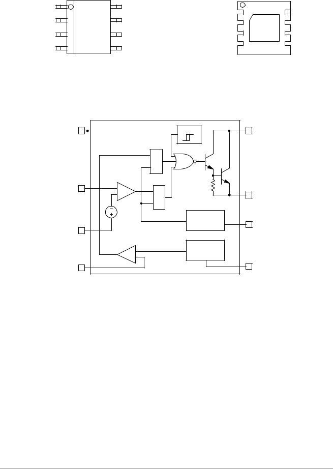
Figure 4. Block Diagram
http://onsemi.com
2

|
|
NCP3063, NCP3063B, NCV3063 |
PIN DESCRIPTION |
|
|
|
|
|
Pin No. |
Pin Name |
Description |
|
|
|
1 |
Switch Collector |
Internal Darlington switch collector |
|
|
|
2 |
Switch Emitter |
Internal Darlington switch emitter |
|
|
|
3 |
Timing Capacitor |
Timing Capacitor |
|
Oscillator Input |
|
|
|
|
4 |
GND |
Ground pin for all internal circuits |
|
|
|
5 |
Comparator |
Inverting input pin of internal comparator |
|
Inverting Input |
|
|
|
|
6 |
VCC |
Voltage Supply |
7 |
Ipk Sense |
Peak Current Sense Input to monitor the voltage drop across an external resistor to limit the peak |
|
|
current through the circuit |
|
|
|
8 |
N.C. |
Pin Not Connected |
|
|
|
Exposed |
Exposed Pad |
The exposed pad beneath the package must be connected to GND (Pin 4). Additionally, using |
Pad |
|
proper layout techniques, the exposed pad can greatly enhance the power dissipation capabilities |
|
|
of the NCP3063. |
|
|
|
MAXIMUM RATINGS (measured vs. Pin 4, unless otherwise noted)
Rating |
Symbol |
Value |
Unit |
|
|
|
|
VCC pin 6 |
VCC |
0 to +40 |
V |
Comparator Inverting Input pin 5 |
VCII |
-0.2 to + VCC |
V |
Darlington Switch Collector pin 1 |
VSWC |
0 to +40 |
V |
Darlington Switch Emitter pin 2 (transistor OFF) |
VSWE |
-0.6 to + VCC |
V |
Darlington Switch Collector to Emitter pin 1-2 |
VSWCE |
0 to +40 |
V |
Darlington Switch Current |
ISW |
1.5 |
A |
Ipk Sense Pin 7 |
VIPK |
-0.2 to VCC + 0.2 |
V |
Timing Capacitor Pin 3 |
VTCAP |
-0.2 to +1.4 |
V |
POWER DISSIPATION AND THERMAL CHARACTERISTICS |
|
|
|
|
|
|
|
Rating |
Symbol |
Value |
Unit |
|
|
|
|
PDIP-8 |
|
|
°C/W |
Thermal Resistance Junction-to-Air |
RqJA |
100 |
|
SOIC-8 |
|
|
°C/W |
Thermal Resistance Junction-to-Air |
RqJA |
180 |
|
DFN-8 |
|
|
°C/W |
Thermal Resistance Junction-to-Air |
RqJA |
80 |
|
Storage Temperature Range |
TSTG |
-65 to +150 |
°C |
Maximum Junction Temperature |
TJ MAX |
+150 |
°C |
Operating Junction Temperature Range (Note 3) |
TJ |
0 to +70 |
°C |
NCP3063 |
|
|
|
NCP3063B, NCV3063 |
|
-40 to +125 |
|
|
|
|
|
Stresses exceeding Maximum Ratings may damage the device. Maximum Ratings are stress ratings only. Functional operation above the Recommended Operating Conditions is not implied. Extended exposure to stresses above the Recommended Operating Conditions may affect device reliability.
1.This device series contains ESD protection and exceeds the following tests:
Pin 1-8: Human Body Model 2000 V per AEC Q100-002; 003 or JESD22/A114; A115Machine Model Method 200 V
2.This device contains latch-up protection and exceeds 100 mA per JEDEC Standard JESD78.
3.The relation between junction temperature, ambient temperature and Total Power dissipated in IC is TJ = TA + Rq • PD
4.The pins which are not defined may not be loaded by external signals
http://onsemi.com
3

NCP3063, NCP3063B, NCV3063
ELECTRICAL CHARACTERISTICS (VCC = 5.0 V, TJ = Tlow to Thigh [Note 5], unless otherwise specified)
Symbol |
Characteristic |
Conditions |
Min |
Typ |
Max |
Unit |
|
|
|
|
|
|
|
OSCILLATOR |
|
|
|
|
|
|
|
|
|
|
|
|
|
fOSC |
Frequency |
(VPin 5 = 0 V, CT = 2.2 nF, |
110 |
150 |
190 |
kHz |
|
|
TJ = 25°C) |
|
|
|
|
IDISCHG / |
Discharge to Charge Current Ratio |
(Pin 7 to VCC, TJ = 25°C) |
5.5 |
6.0 |
6.5 |
- |
ICHG |
|
|
|
|
|
|
IDISCHG |
Capacitor Discharging Current |
(Pin 7 to VCC, TJ = 25°C) |
|
1650 |
|
mA |
ICHG |
Capacitor Charging Current |
(Pin 7 to VCC, TJ = 25°C) |
|
275 |
|
mA |
VIPK(Sense) |
Current Limit Sense Voltage |
(TJ = 25°C) (Note 6) |
165 |
200 |
235 |
mV |
OUTPUT SWITCH (Note 7) |
|
|
|
|
|
|
|
|
|
|
|
|
|
VSWCE(DROP) |
Darlington Switch Collector to |
(ISW = 1.0 A, Pin 2 to GND, |
|
1.0 |
1.3 |
V |
|
Emitter Voltage Drop |
TJ = 25°C) (Note 7) |
|
|
|
|
IC(OFF) |
Collector Off-State Current |
(VCE = 40 V) |
|
0.01 |
100 |
mA |
COMPARATOR |
|
|
|
|
|
|
|
|
|
|
|
|
|
VTH |
Threshold Voltage |
TJ = 25°C |
|
1.250 |
|
V |
|
|
NCP3063 |
-1.5 |
|
+1.5 |
% |
|
|
|
|
|
|
|
|
|
NCP3063B, NCV3063 |
-2 |
|
+2 |
% |
|
|
|
|
|
|
|
REGLiNE |
Threshold Voltage Line Regulation |
(VCC = 5.0 V to 40 V) |
-6.0 |
2.0 |
6.0 |
mV |
ICII in |
Input Bias Current |
(Vin = Vth) |
-1000 |
-100 |
1000 |
nA |
TOTAL DEVICE |
|
|
|
|
|
|
|
|
|
|
|
|
|
ICC |
Supply Current |
(VCC = 5.0 V to 40 V, |
|
|
7.0 |
mA |
|
|
CT = 2.2 nF, Pin 7 = VCC, |
|
|
|
|
|
|
VPin 5 > Vth, Pin 2 = GND, |
|
|
|
|
|
|
remaining pins open) |
|
|
|
|
|
|
|
|
|
|
|
|
Thermal Shutdown Threshold |
|
|
160 |
|
°C |
|
|
|
|
|
|
|
|
Hysteresis |
|
|
10 |
|
°C |
|
|
|
|
|
|
|
5.NCP3063: Tlow = 0°C, Thigh = +70°C;
NCP3063B, NCV3063: Tlow = -40°C, Thigh = +125°C
6.The VIPK(Sense) Current Limit Sense Voltage is specified at static conditions. In dynamic operation the sensed current turn-off value depends on comparator response time and di/dt current slope. See the Operating Description section for details.
7.Low duty cycle pulse techniques are used during test to maintain junction temperature as close to ambient temperature as possible.
8.NCV prefix is for automotive and other applications requiring site and change control.
http://onsemi.com
4

|
|
|
|
|
|
|
|
|
|
NCP3063, NCP3063B, NCV3063 |
|
|
|
|
|
|
||||
|
450 |
|
|
|
|
|
|
|
|
|
|
190 |
|
|
|
|
|
|
|
|
|
400 |
|
|
|
|
|
|
|
|
|
|
180 |
|
|
|
|
|
|
CT = 2.2 nF |
|
|
|
|
|
|
|
|
|
|
|
|
|
|
|
|
|
|
|
TJ = 25°C |
||
|
350 |
|
|
|
|
|
|
|
|
|
|
|
|
|
|
|
|
|
||
(kHz) |
|
|
|
|
|
|
|
|
|
|
170 |
|
|
|
|
|
|
|
|
|
|
|
|
|
|
|
|
|
|
|
(Hz) |
|
|
|
|
|
|
|
|
||
300 |
|
|
|
|
|
|
|
|
|
160 |
|
|
|
|
|
|
|
|
||
|
|
|
|
|
|
|
|
|
|
|
|
|
|
|
|
|
|
|||
FREQUENCY |
250 |
|
|
|
|
|
|
|
|
|
FREQUENCY |
|
|
|
|
|
|
|
|
|
|
|
|
|
|
|
|
|
|
|
|
|
|
|
|
|
|
|
|||
200 |
|
|
|
|
|
|
|
|
|
150 |
|
|
|
|
|
|
|
|
||
|
|
|
|
|
|
|
|
|
|
|
|
|
|
|
|
|
|
|||
150 |
|
|
|
|
|
|
|
|
|
140 |
|
|
|
|
|
|
|
|
||
|
|
|
|
|
|
|
|
|
|
|
|
|
|
|
|
|
|
|||
100 |
|
|
|
|
|
|
|
|
|
130 |
|
|
|
|
|
|
|
|
||
|
|
|
|
|
|
|
|
|
|
|
|
|
|
|
|
|
|
|
||
|
50 |
|
|
|
|
|
|
|
|
|
|
120 |
|
|
|
|
|
|
|
|
|
0 |
|
|
|
|
|
|
|
|
|
|
110 |
7 |
12 |
16 |
21 |
25 |
29 |
34 |
38 40 |
|
0 |
1 |
2 |
3 |
4 |
5 |
6 |
7 |
8 |
9 1011 121314 15161718 1920 |
|
3 |
||||||||
|
|
|
|
|
|
|
|
|
|
|
||||||||||
VOLTAGE DROP (V)
Ct, CAPACITANCE (nF)
Figure 5. Oscillator Frequency vs. Oscillator
Timing Capacitor
2.4 |
|
|
|
|
|
|
|
|
|
|
|
|
1.25 |
|
|
|
|
|
|
|
|
|
|
|
|
|
|
||
2.2 |
|
|
|
|
|
|
VCC = 5.0 V |
|
|
|
|
|
||
|
|
|
|
|
|
|
|
|
|
|
||||
|
|
|
|
|
|
|
IE = 1 A |
|
|
(V) |
1.20 |
|
||
2.0 |
|
|
|
|
|
|
|
|
|
|
|
|
|
|
|
|
|
|
|
|
|
|
|
|
|
|
|
||
1.8 |
|
|
|
|
|
|
|
|
|
|
|
DROP |
1.15 |
|
|
|
|
|
|
|
|
|
|
|
|
VOLTAGE |
|
|
|
1.6 |
|
|
|
|
|
|
|
|
|
|
|
1.10 |
|
|
|
|
|
|
|
|
|
|
|
|
|
|
|
||
|
|
|
|
|
|
|
|
|
|
|
|
|
|
|
1.4 |
|
|
|
|
|
|
|
|
|
|
|
|
1.05 |
|
|
|
|
|
|
|
|
|
|
|
|
|
|
||
1.2 |
|
|
|
|
|
|
|
|
|
|
|
|
|
|
|
|
|
|
|
|
|
|
|
|
|
|
|
|
|
|
|
|
|
|
|
|
|
|
|
|
|
|
|
|
1.0 |
|
|
|
|
|
|
|
|
|
|
|
|
1.0 |
|
-50 |
0 |
50 |
|
100 |
|
150 |
|
-50 |
||||||
TJ, JUNCTION TEMPERATURE (°C)
VCC, SUPPLY VOLTAGE (V)
Figure 6. Oscillator Frequency vs. Supply Voltage
VCC = 5.0 V
IC = 1 A
0 |
50 |
100 |
150 |
TJ, JUNCTION TEMPERATURE (°C)
Figure 7. Emitter Follower Configuration Output Darlington Switch Voltage Drop vs. Temperature
Figure 8. Common Emitter Configuration Output Darlington Switch Voltage Drop vs. Temperature
VOLTAGE DROP (V)
2.0
1.9VCC = 5.0 V
1.8 |
TJ = 25°C |
|
|
1.7 |
|
|
|
1.6 |
|
|
|
1.5 |
|
|
|
1.4 |
|
|
|
1.3 |
|
|
|
1.2 |
|
|
|
1.1 |
|
|
|
1.0 |
|
|
|
0 |
0.5 |
1.0 |
1.5 |
IE, EMITTER CURRENT (A)
Figure 9. Emitter Follower Configuration Output Darlington Switch Voltage Drop vs. Emitter Current
VOLTAGE DROP (V)
1.5 |
|
|
|
1.4 |
|
|
VCC = 5.0 V |
|
|
|
|
1.3 |
|
|
TJ = 25°C |
1.2 |
|
|
|
1.1 |
|
|
|
1.0 |
|
|
|
0.9 |
|
|
|
0.8 |
|
|
|
0.7 |
|
|
|
0.6 |
|
|
|
0.5 |
|
|
|
0 |
0.5 |
1.0 |
1.5 |
IC, COLLECTOR CURRENT (A)
Figure 10. Common Emitter Configuration Output Darlington Switch Voltage Drop vs.
Collector Current
http://onsemi.com
5

NCP3063, NCP3063B, NCV3063
Vth, COMPARATOR THRESHOLD VOLTAGE (V)
1.30
1.28
1.26
1.24
1.22
1.20
-40 -25 -10 5 20 35 50 65 80 95 110 125 TJ, JUNCTION TEMPERATURE (°C)
VOLTAGE (V)
Vipk(sense), CURRENT LIMIT SENSE
0.30
0.28
0.26
0.24
0.22
0.20
0.18
0.16
0.14
0.12
0.10
-40 -25 -10 5 20 35 50 65 80 95 110 125 TJ, JUNCTION TEMPERATURE (°C)
Figure 11. Comparator Threshold Voltage vs. |
Figure 12. Current Limit Sense Voltage vs. |
Temperature |
Temperature |
ICC, SUPPLY CURRENT (mA)
6.0 |
|
|
|
|
|
|
|
|
|
|
|
|
|
|
|
|
|
|
|
|
|
|
|
|
|
|
|
|
|
|
|
|
|
|
|
5.5 |
|
|
|
|
|
|
|
|
|
|
|
|
|
|
|
|
|
5.0 |
|
|
|
|
|
|
|
|
|
|
|
|
|
|
|
|
|
4.5 |
|
|
|
|
|
|
|
|
|
|
|
|
|
|
|
|
|
4.0 |
|
|
|
|
|
|
|
|
|
|
|
|
|
|
|
|
|
3.5 |
|
|
|
|
|
|
|
|
|
|
|
|
|
|
|
|
|
|
|
|
|
|
|
|
|
|
|
|
|
|
|
|
|
|
|
3.0 |
|
|
|
|
|
|
|
|
|
|
|
CT = 2.2 nF |
|
|
|||
2.5 |
|
|
|
|
|
|
|
|
|
|
|
Pin 5, 7 = VCC |
|
|
|||
|
|
|
|
|
|
|
|
|
|
|
Pin 2 = GND |
|
|
||||
2.0 |
|
|
|
|
|
|
|
|
|
|
|
|
|
|
|
|
|
3.0 |
8.0 |
13 |
18 |
23 |
28 |
33 |
38 |
43 |
|||||||||
VCC, SUPPLY VOLTAGE (V)
Figure 13. Standby Supply Current vs. Supply Voltage
http://onsemi.com
6
 Loading...