


DTC124ERLRP
ON Semiconductor DTC124ERLRP, DTC124ERLRM, DTC124ERLRA, DTC143ZRLRP, DTC143ZRLRM Datasheet
...
Semiconductor Components Industries, LLC, 2000
May, 2000 – Rev. 0
1 Publication Order Number:
DTC114E/D
DTC114E SERIES
Preferred Devices
Bias Resistor Transistor
NPN Silicon Surface Mount Transistor
with Monolithic Bias Resistor Network
This new series of digital transistors is designed to replace a single
device and its external resistor bias network. The BRT (Bias Resistor
Transistor) contains a single transistor with a monolithic bias network
consisting of two resistors; a series base resistor and a base–emitter
resistor. The BRT eliminates these individual components by
integrating them into a single device. The use of a BRT can reduce
both system cost and board space. The device is housed in the TO–92
package which is designed for through hole applications.
MAXIMUM RATINGS (T
A
= 25°C unless otherwise noted)
Rating Symbol Value Unit
Collector-Base Voltage V
CBO
50 Vdc
Collector-Emitter Voltage V
CEO
50 Vdc
Collector Current I
C
100 mAdc
Total Power Dissipation
@ T
A
= 25°C
(1.)
Derate above 25°C
P
D
350
2.81
mW
mW/°C
THERMAL CHARACTERISTICS
Characteristic Symbol Value Unit
Thermal Resistance, Junction to
Ambient (surface mounted)
R
θ
JA
357 °C/W
Operating and Storage
T emperature Range
TJ, T
stg
–55 to
+150
°C
Maximum Temperature for
Soldering Purposes,
Time in Solder Bath
T
L
260
10
°C
Sec
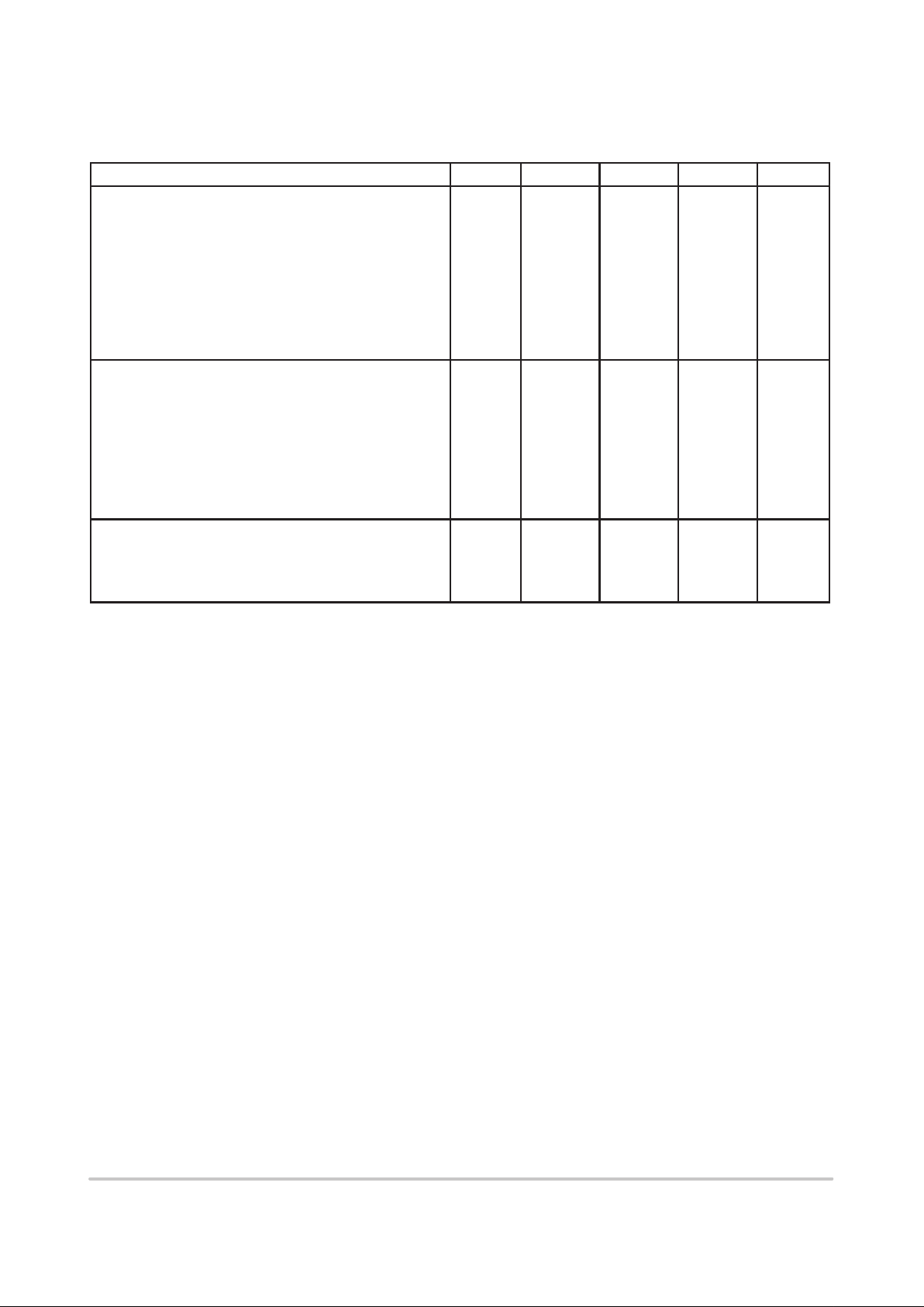
DEVICE MARKING AND RESISTOR VALUES
Device Marking R1 (K) R2 (K) Shipping
DTC114E
DTC124E
DTC144E
DTC114Y
DTC114T
DTC143T
DTD113E
DTC123E
DTC143E
DTC143Z
DTC114E
DTC124E
DTC144E
DTC114Y
DTC114T
DTC143T
DTD113E
DTC123E
DTC143E
DTC143Z
10
22
47
10
10
4.7
1.0
2.2
4.7
4.7
10
22
47
47
∞
∞
1.0
2.2
4.7
47
5000/Box
1. Device mounted on a FR–4 glass epoxy printed circuit board using the
minimum recommended footprint.
http://onsemi.com
CASE 29
TO–92 (TO–226)
STYLE 1
Preferred devices are recommended choices for future use
and best overall value.
NPN SILICON
BIAS RESISTOR
TRANSISTOR
1
2
3
COLLECTOR
3
2
BASE
1
EMITTER

DTC114E SERIES
http://onsemi.com
2
ELECTRICAL CHARACTERISTICS (T
A
= 25°C unless otherwise noted)
Characteristic
Symbol Min Typ Max Unit
OFF CHARACTERISTICS
Collector–Base Cutoff Current (VCB = 50 V, IE = 0) I
CBO
— — 100 nAdc
Collector–Emitter Cutoff Current (VCE = 50 V, IB = 0) I
CEO
— — 500 nAdc
Emitter–Base Cutoff Current DTC114E
(V
EB
= 6.0 V, IC = 0) DTC124E
DTC144E
DTC114Y
DTC114T
DTC143T
DTD113E
DTC123E
DTC143E
DTC143Z
I
EBO
—
—
—
—
—
—
—
—
—
—
—
—
—
—
—
—
—
—
—
—
0.5
0.2
0.1
0.2
0.9
1.9
4.3
2.3
1.5
0.18
mAdc
Collector–Base Breakdown Voltage (IC = 10 µA, IE = 0) V
(BR)CBO
50 — — Vdc
Collector–Emitter Breakdown Voltage
(2.)
(IC = 2.0 mA, IB = 0) V
(BR)CEO
50 — — Vdc
ON CHARACTERISTICS
(2.)
DC Current Gain DTC114E
(V
CE
= 10 V, IC = 5.0 mA) DTC124E
DTC144E
DTC114Y
DTC114T
DTC143T
DTD113E
DTC123E
DTC143E
DTC143Z
h
FE
35
60
80
80
160
160
3.0
8.0
15
80
60
100
140
140
350
350
5.0
15
30
200
—
—
—
—
—
—
—
—
—
—
Collector–Emitter Saturation Voltage
(I
C
= 10 mA, IE = 0.3 mA) DTC144E/DTC114Y
(I
C
= 10 mA, IB = 0.3 mA) DTD113E/DTC143E
(I
C
= 10 mA, IB = 5 mA) DTC123E
(I
C
= 10 mA, IB = 1 mA) DTC114T/DTC143T/
(I
C
= 10 mA, IB = 1 mA) DTC143Z/DTC124E
V
CE(sat)
— — 0.25 Vdc
Output Voltage (on)
(V
CC
= 5.0 V, VB = 2.5 V, RL = 1.0 kΩ) DTC114E
DTC124E
DTC114Y
DTC114T
DTC143T
DTD113E
DTC123E
DTC143E
DTC143Z
(V
CC
= 5.0 V, VB = 3.5 V, RL = 1.0 kΩ) DTC144E
V
OL
—
—
—
—
—
—
—
—
—
—
—
—
—
—
—
—
—
—
—
—
0.2
0.2
0.2
0.2
0.2
0.2
0.2
0.2
0.2
0.2
Vdc
2. Pulse Test: Pulse Width < 300 µs, Duty Cycle < 2.0%
DTC114E SERIES
http://onsemi.com
3
ELECTRICAL CHARACTERISTICS (T
A
= 25°C unless otherwise noted) (Continued)
Characteristic
Symbol Min Typ Max Unit
Output Voltage (of f)
(V
CC
= 5.0 V, VB = 0.5 V, RL = 1.0 kΩ) DTC114E
DTC124E
DTC144E
DTC114Y
DTC123E
DTC143E
(V
CC
= 5.0 V, VB = 0.05 V, RL = 1.0 kΩ) DTD113E
(V
CC
= 5.0 V, VB = 0.25 V, RL = 1.0 kΩ) DTC114T
DTC143T
DTC143Z
V
OH
4.9 — — Vdc
Input Resistor DTC114E
DTC124E
DTC144E
DTC114Y
DTC114T
DTC143T
DTD113E
DTC123E
DTC143E
DTC143Z
R1 7.0
15.4
32.9
7.0
7.0
3.3
0.7
1.5
3.3
3.3
10
22
47
10
10
4.7
1.0
2.2
4.7
4.7
13
28.6
61.1
13
13
6.1
1.3
2.9
6.1
6.1
kΩ
Resistor Ratio DTC114E/DTC124E/DTC144E
DTC114Y
DTC114T/DTC143T
DTD113E/DTC123E/DTC143E
DTC143Z
R1/R
2
0.8
0.17
—
0.8
0.055
1.0
0.21
—
1.0
0.1
1.2
0.25
—
1.2
0.185

DTC114E SERIES
http://onsemi.com
4
TYPICAL ELECTRICAL CHARACTERISTICS
DTC114E
1002030
IC, COLLECTOR CURRENT (mA)
10
1
0.1
V
in
, INPUT VOLTAGE (VOLTS)
TA= –25°C
75°C
25°C
40
50
1
0.1
0.01
0.001
020 406080
I
C
, COLLECTOR CURRENT (mA)
V
CE(sat)
, MAXIMUM COLLECTOR VOLTAGE (VOLTS)
1000
100
10
1 10 100
I
C
, COLLECTOR CURRENT (mA)
h
FE
,
D
C
C
U
RRE
N
T
G
AI
N (N
ORMALI
Z
E
D)
TA=75°C
25°C
–25°C
TA= –25°C
25°C
IC/IB = 10
75°C
25°C
TA= –25°C
100
10
1
0.1
0.01
0.001
01234
V
in
, INPUT VOLTAGE (VOLTS)
I
C
,
COLLECTOR
C
U
RRE
N
T
(m
A
)
5678910
50
010203040
4
3
1
2
0
V
R
, REVERSE BIAS VOLTAGE (VOLTS)
C
ob
, CAPACITANCE (pF)
75°C
f = 1 MHz
l
E
= 0 V
T
A
= 25°C
VO = 5 V
VCE = 10 V
V
O
= 0.2 V
Figure 1. Derating Curve
250
200
150
100
50
0
–50 0 50 100 150
T
A
, AMBIENT TEMPERATURE (°C)
P
D
,
P
O
W
ER
D
ISSI
P
ATIO
N (
MILLI
W
ATTS
)
R
θ
JA
= 625°C/W
Figure 2. V
CE(sat)
versus I
C
Figure 3. DC Current Gain
Figure 4. Output Capacitance
Figure 5. V
CE(sat)
versus I
C
Figure 6. V
CE(sat
)
versus I
C
 Loading...