


MC1489, MC1489A
Quad Line EIA-232D
Receivers
The MC1489 monolithic quad line receivers are designed to interface data terminal equipment with data communications equipment in conformance with the specifications of EIA Standard No. EIA−232D.
Features
•Input Resistance − 3.0 k to 7.0 k
•Input Signal Range − ± 30 V
•Input Threshold Hysteresis Built In
•Response Control
a)Logic Threshold Shifting
b)Input Noise Filtering
•Pb−Free Packages are Available
Line Driver |
Interconnecting |
|
|
Line Receiver |
|||||
MC1488 |
Cable |
|
|
|
MC1489 |
||||
|
|
|
|
|
|
|
|
|
|
|
|
|
|
|
|
|
|
|
|
|
|
|
|
|
|
|
|
|
|
|
|
|
|
|
|
|
|
|
|
|
|
|
|
|
|
|
|
|
|
MDTL Logic Input |
Interconnecting |
MDTL Logic Output |
|
Cable |
|||
|
|
Figure 1. Simplified Application
|
http://onsemi.com |
|
SOIC−14 |
14 |
D SUFFIX |
CASE 751A
1
PDIP−14
P SUFFIX
CASE 646
14
1
SOEIAJ−14
14  M SUFFIX
CASE 965
1
PIN CONNECTIONS
Input A |
1 |
|
Response |
2 |
|
Control A |
||
|
||
Output A |
3 |
|
Input B |
4 |
|
Response |
5 |
|
Control B |
||
|
||
Output B |
6 |
|
Ground |
7 |
14 |
VCC |
|
13 |
Input D |
|
12 |
Response |
|
|
Control D |
|
11 |
Output D |
|
10 |
Input C |
|
9 |
Response |
|
Control C |
||
|
||
8 |
Output C |
ORDERING INFORMATION
See detailed ordering and shipping information in the package dimensions section on page 8 of this data sheet.
DEVICE MARKING INFORMATION
See general marking information in the device marking section on page 8 of this data sheet.
*For additional information on our Pb−Free strategy and soldering details, please download the
ON Semiconductor Soldering and Mounting Techniques Reference Manual, SOLDERRM/D.
Semiconductor Components Industries, LLC, 2004 |
1 |
Publication Order Number: |
April, 2004 − Rev. 8 |
|
MC1489/D |
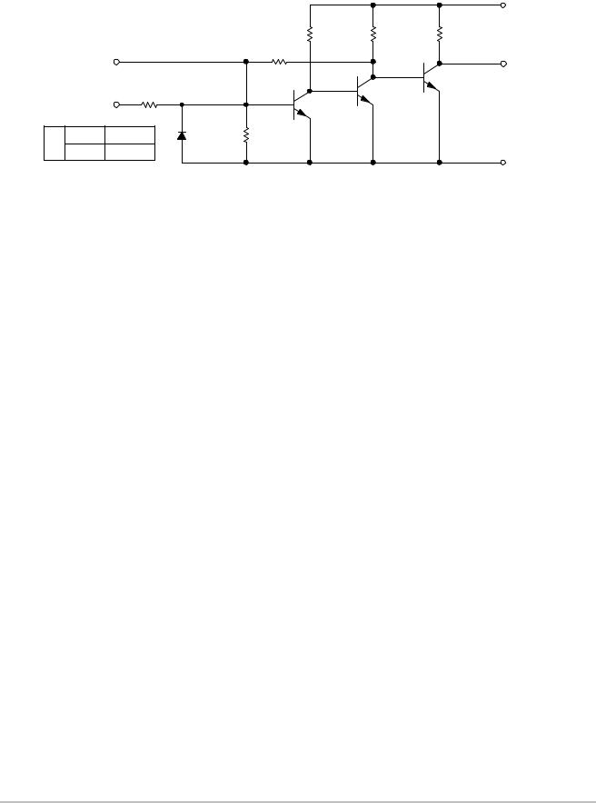
MC1489, MC1489A
14
|
|
|
|
VCC |
|
|
9.0 k |
5.0 k |
1.7 k |
|
|
RF |
|
|
Response Control 2 |
|
|
|
3 Output |
|
|
|
|
|
|
3.8 k |
|
|
|
Input 1 |
|
|
|
|
MC1489 |
MC1489A |
10 k |
|
|
RF 6.7 k |
1.6 k |
|
|
|
|
|
|
|
7 GND |
Figure 2. Representative Schematic Diagram
(1/4 of Circuit Shown)
http://onsemi.com
2

MC1489, MC1489A
MAXIMUM RATINGS (TA = + 25°C, unless otherwise noted)
Rating |
Symbol |
Value |
Unit |
|
|
|
|
Power Supply Voltage |
VCC |
10 |
Vdc |
Input Voltage Range |
VIR |
± 30 |
Vdc |
Output Load Current |
IL |
20 |
mA |
Power Dissipation (Package Limitation, SOIC−14 and Plastic Dual In−Line Package) |
PD |
1000 |
mW |
Derate above TA = + 25°C |
1/ JA |
6.7 |
mW/°C |
Operating Ambient Temperature Range |
TA |
0 to + 75 |
°C |
Storage Temperature Range |
Tstg |
− 65 to + 175 |
°C |
Maximum ratings are those values beyond which device damage can occur. Maximum ratings applied to the device are individual stress limit values (not normal operating conditions) and are not valid simultaneously. If these limits are exceeded, device functional operation is not implied, damage may occur and reliability may be affected.
ELECTRICAL CHARACTERISTICS (Response control pin is open.) (VCC = + 5.0 Vdc ± 10%, TA = 0 to + 75°C, unless otherwise noted)
Characteristics |
|
Symbol |
Min |
Typ |
Max |
Unit |
|
|
|
|
|
|
|
|
|
Positive Input Current |
|
(VIH = + 25 Vdc) |
IIH |
3.6 |
− |
8.3 |
mA |
|
|
(VIH = + 3.0 Vdc) |
|
0.43 |
− |
− |
|
Negative Input Current |
|
(VIH = − 25 Vdc) |
IIL |
− 3.6 |
− |
− 8.3 |
mA |
|
|
(VIH = − 3.0 Vdc) |
|
− 0.43 |
− |
− |
|
Input Turn−On Threshold Voltage |
|
|
VIH |
|
|
|
Vdc |
(TA = + 25°C, VOL 0.45 V) |
|
MC1489 |
|
1.0 |
− |
1.5 |
|
|
|
MC1489A |
|
1.75 |
1.95 |
2.25 |
|
|
|
|
|
|
|
|
|
Input Turn−Off Threshold Voltage |
|
|
VIL |
|
|
|
Vdc |
(TA = + 25°C, VOH 2.5 V, IL = − 0.5 mA) |
MC1489 |
|
0.75 |
− |
1.25 |
|
|
|
|
MC1489A |
|
0.75 |
0.8 |
1.25 |
|
|
|
|
|
|
|
|
|
Output Voltage High |
(VIH = 0.75 V, IL = − 0.5 mA) |
VOH |
2.5 |
4.0 |
5.0 |
Vdc |
|
|
(Input Open Circuit, IL = − 0.5 mA) |
|
2.5 |
4.0 |
5.0 |
|
|
Output Voltage Low |
(VIL = 3.0 V, IL = 10 mA) |
VOL |
− |
0.2 |
0.45 |
Vdc |
|
Output Short−Circuit Current |
|
|
IOS |
− |
− 3.0 |
− 4.0 |
mA |
Power Supply Current (All Gates ªon,º I = 0 mA, V |
= + 5.0 Vdc) |
I |
− |
16 |
26 |
mA |
|
|
out |
IH |
CC |
|
|
|
|
Power Consumption |
(VIH = + 5.0 Vdc) |
PC |
− |
80 |
130 |
mW |
|
SWITCHING CHARACTERISTICS (VCC = 5.0 Vdc ± 1%, TA = + 25°C, See Figure 3.) |
|
|
|
|
|||
Propagation Delay Time |
(RL = 3.9 k ) |
tPLH |
− |
25 |
85 |
ns |
|
Rise Time |
(RL = 3.9 k ) |
tTLH |
− |
120 |
175 |
ns |
|
Propagation Delay Time |
(RL = 390 k ) |
tPHL |
− |
25 |
50 |
ns |
|
Fall Time |
(RL = 390 k ) |
tTHL |
− |
10 |
20 |
ns |
|
http://onsemi.com
3
 Loading...