


ON Semiconductor BC489BRL1, BC489B, BC489AZL1, BC489A, BC489 Datasheet
...
MOTOROLA
SEMICONDUCTOR TECHNICAL DATA
Order this document by BC489/D
High Current Transistors
NPN Silicon
|
|
|
|
COLLECTOR |
|||
|
|
|
|
1 |
|
||
|
|
2 |
|
|
|
|
|
|
|
|
|
|
|
|
|
|
|
|
|
|
|
|
|
|
|
BASE |
|
|
|
|
|
|
|
|
|
|
|
||
|
|
|
|
3 |
|||
MAXIMUM RATINGS |
|
|
|
|
EMITTER |
||
|
|
|
|
|
|
|
|
|
|
|
|
|
|
|
|
Rating |
Symbol |
Value |
|
Unit |
|||
|
|
|
|
|
|
|
|
Collector± Emitter Voltage |
VCEO |
80 |
|
|
Vdc |
||
Collector± Base Voltage |
VCBO |
80 |
|
|
Vdc |
||
Emitter± Base Voltage |
VEBO |
5.0 |
|
|
Vdc |
||
Collector Current Ð Continuous |
IC |
0.5 |
|
|
Adc |
||
Total Device Dissipation @ TA = 25°C |
PD |
625 |
|
|
mW |
||
Derate above 25°C |
|
5.0 |
|
|
mW/°C |
||
|
|
|
|
|
|
|
|
Total Device Dissipation @ TC = 25°C |
PD |
1.5 |
|
|
Watt |
||
Derate above 25°C |
|
12 |
|
|
mW/°C |
||
|
|
|
|
|
|
|
|
Operating and Storage Junction |
TJ, Tstg |
± 55 to +150 |
|
°C |
|||
Temperature Range |
|
|
|
|
|
|
|
|
|
|
|
|
|
|
|
THERMAL CHARACTERISTICS |
|
|
|
|
|
|
|
|
|
|
|
|
|
|
|
Characteristic |
Symbol |
Max |
|
Unit |
|||
|
|
|
|
|
|
|
|
Thermal Resistance, Junction to Ambient |
RqJA |
200 |
|
|
°C/W |
||
Thermal Resistance, Junction to Case |
RqJC |
83.3 |
|
|
°C/W |
||
ELECTRICAL CHARACTERISTICS (TA = 25°C unless otherwise noted)
BC489,A,B
1
2 3
CASE 29±04, STYLE 17 TO±92 (TO±226AA)
Characteristic |
Symbol |
Min |
Typ |
Max |
Unit |
|
|
|
|
|
|
OFF CHARACTERISTICS
Collector± Emitter Breakdown Voltage(1) |
|
V(BR)CEO |
80 |
Ð |
Ð |
Vdc |
(IC = 10 mAdc, IB = 0) |
|
|
|
|
|
|
Collector± Base Breakdown Voltage |
|
V(BR)CBO |
80 |
Ð |
Ð |
Vdc |
(IC = 100 mAdc, IE = 0) |
|
|
|
|
|
|
Emitter± Base Breakdown Voltage |
|
V(BR)EBO |
5.0 |
Ð |
Ð |
Vdc |
(IE = 10 mAdc, IC = 0) |
|
|
|
|
|
|
Collector Cutoff Current |
|
ICBO |
Ð |
Ð |
100 |
nAdc |
(VCB = 60 Vdc, IE = 0) |
|
|
|
|
|
|
ON CHARACTERISTICS* |
|
|
|
|
|
|
|
|
|
|
|
|
|
DC Current Gain |
|
hFE |
|
|
|
Ð |
(IC = 10 mAdc, VCE = 2.0 Vdc) |
|
|
40 |
Ð |
Ð |
|
(IC = 100 mAdc, VCE = 2.0 Vdc) |
BC489 |
|
60 |
Ð |
400 |
|
|
BC489A |
|
100 |
160 |
250 |
|
|
BC489B |
|
160 |
260 |
400 |
|
(IC = 1.0 Adc, VCE = 5.0 Vdc)* |
|
|
15 |
Ð |
Ð |
|
1. Pulse Test: Pulse Width = 300 ms, Duty Cycle 2%.
Motorola, Inc. 1996
BC489,A,B
ELECTRICAL CHARACTERISTICS (TA = 25°C unless otherwise noted) (Continued)
Characteristic |
Symbol |
Min |
Typ |
Max |
Unit |
|
|
|
|
|
|
ON CHARACTERISTICS* (Continued)
Collector± Emitter Saturation Voltage |
VCE(sat) |
|
|
|
Vdc |
(IC = 500 mAdc, IB = 50 mAdc) |
|
Ð |
0.2 |
0.5 |
|
(IC = 1.0 Adc, IB = 100 mAdc) |
|
Ð |
0.3 |
Ð |
|
Base ± Emitter Saturation Voltage |
VBE(sat) |
|
|
|
Vdc |
(IC = 500 mAdc, IB = 50 mAdc) |
|
Ð |
0.85 |
1.2 |
|
(IC = 1.0 Adc, IB = 100 mAdc)(1) |
|
Ð |
0.9 |
Ð |
|
DYNAMIC CHARACTERISTICS |
|
|
|
|
|
|
|
|
|
|
|
Current±Gain Ð Bandwidth Product |
fT |
Ð |
200 |
Ð |
MHz |
(IC = 50 mAdc, VCE = 2.0 Vdc, f = 100 MHz) |
|
|
|
|
|
Output Capacitance |
Cob |
Ð |
7.0 |
Ð |
pF |
(VCB = 10 Vdc, IE = 0, f = 1.0 MHz) |
|
|
|
|
|
Input Capacitance |
Cib |
Ð |
50 |
Ð |
pF |
(VEB = 0.5 Vdc, IC = 0, f = 1.0 MHz) |
|
|
|
|
|
1. Pulse Test: Pulse Width = 300 ms, Duty Cycle 2.0%. |
|
|
|
|
|
|
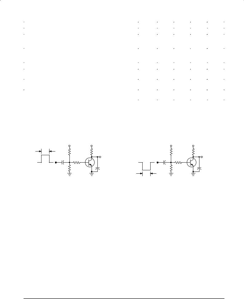
TURN±ON TIME |
|
TURN±OFF TIME |
|
||
|
±1.0 V |
VCC |
+VBB |
VCC |
||
5.0 μs |
|
+40 V |
|
|
+40 V |
|
+10 V |
100 |
RL |
|
100 |
RL |
|
RB |
OUTPUT |
Vin |
RB |
OUTPUT |
||
Vin |
||||||
|
|
|||||
0 |
|
|
|
|
|
|
tr = 3.0 ns |
5.0 μF 100 |
*C < 6.0 pF |
5.0 μF |
100 |
*C < 6.0 pF |
|
|
|
S |
|
|
S |
|
5.0 μs tr = 3.0 ns
*Total Shunt Capacitance of Test Jig and Connectors For PNP Test Circuits, Reverse All Voltage Polarities
Figure 1. Switching Time Test Circuits
2 |
Motorola Small±Signal Transistors, FETs and Diodes Device Data |
 Loading...