Fairchild Semiconductor KA2142 Datasheet

www.fairchildsemi.com
KA2142C
Vertical Deflection Output Circuit
Features |
Description |
|
• |
High output current |
The KA2142C is a monolithic linear IC designed for color |
• |
Pump - up circuit |
TV and monitor vertical deflection output. It is intended for |
• |
Low dissipation |
direct drive of the deflection coils with a high efficiency. |
•Minimum number of external parts required
•Direct drive to the deflectin coils
• Internal thermal shutdown circuit |
10-SIP H/S |
Applications
•Power Amplifier
•Thermal Protection
•Flyback Generator
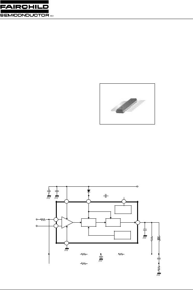
Internal Block Diagram
|
+ |
|
|
|
Vcc(L) |
|
|
|
|
|
|
|
|
|
Vcc(H) |
+ |
|
|
|
|
|
|
|
|
|
2 |
9 |
4 |
|
|
|
|
|
FLYBACK |
|
|
|
|
|
GENERATOR |
|
Sawtooth IN |
1 |
+PRE |
|
|
|
|
DRIVE |
OUTPUT |
6 |
||
Vref |
10 |
-AMP |
STAGE |
STAGE |
|
|
|
|
|
THERMAL |
|
|
|
|
|
SHUTDOWN |
D.Y |
|
|
|
|
|
|
|
|
5 |
|
|
|
|
|
|
|
+ |
+ |
|
|
|
|
|
Rev. 1.0.0
©2001 Fairchild Semiconductor Corporation

KA2142C
Pin Assignments
|
|
KA2142AC |
|
|
||
1 |
2 |
3 |
4 |
5 |
6 |
7 |
Pin Number |
Symbol |
I/O |
Pin Function Descrition |
1 |
Vin ( - ) |
I |
Inverting Input |
|
|
|
|
2 |
Vcc(L) |
I |
Supply Voltage |
|
|
|
|
3 |
- |
- |
N.C. |
|
|
|
|
4 |
F.G |
O |
Flyback Generator |
|
|
|
|
5 |
GND |
- |
Ground |
|
|
|
|
6 |
VO |
O |
Output |
|
|
|
|
7 |
- |
- |
N.C. |
|
|
|
|
8 |
- |
- |
N.C. |
|
|
|
|
9 |
Vcc(H) |
I |
Output Stage Supply Voltage |
|
|
|
|
10 |
Vin ( + ) |
I |
Non-Inverting Input |
|
|
|
|
2

KA2142C
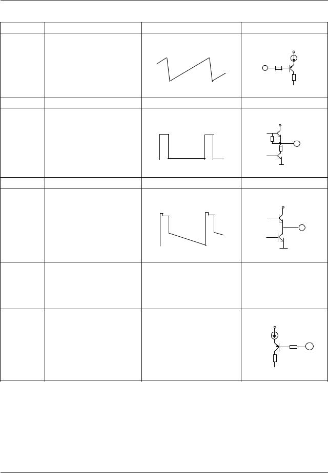
Pin Definitions
Pin Number |
Pin Name |
Waveform |
Equivalent Circuit |
|
|
|
vcc |
1 |
Inverting Input |
|
1 |
|
|
|
|
2 |
Voltage Supply |
DC |
- |
|
|
|
vCC |
4 |
Flyback Generator |
|
4 |
5 |
Ground |
DC |
- |
|
|
|
vCC |
6 |
Output Voltage |
|
6 |
|
|
|
2Vs |
||||||
9 |
Output Stage Voltage Supply |
|
|
|
|
|
- |
||
|
Vs |
|
|
|
|||||
|
|
|
|
|
|
|
|||
vcc
10 |
Non-Inverting Input |
DC |
10 |
3

KA2142C
Absolute Maximum Rating ( Ta = 25oC )
Parameter |
Symbol |
Value |
Unit |
|
Supply Voltage |
Vcc(L) |
35 |
V |
|
|
|
|
|
|
Flyback Peak Voltage |
V6, V9 |
70 |
V |
|
|
|
|
|
|
Flyback Generator Voltage |
V6 |
35 |
V |
|
|
|
|
|
|
Input Voltage |
V1, V10 |
V cc(L) - 0.5 |
V |
|
|
|
|
|
|
Peak - to - Peak Output Current* |
Io(p-p) |
3 |
A |
|
|
|
|
|
|
Peak - to - Peak Flyback Current |
I4(p-p) |
3 |
A |
|
( f = 50 or 60Hz, Tfb ≤ 1.5mS ) |
||||
|
|
|
||
Total Power Dissipation ( Ta = 25oC ) |
PD |
15 |
W |
|
Storage Temperature Range |
Tstg |
-40 ~ +150 |
oC |
|
Operating Ambient Temperature |
Topt |
-25 ~ +70 |
oC |
* Maximum output peak to peak current in TV or Monitor set.
Thermal Data
Parameter |
Symbol |
Value |
Unit |
Thermal Resistance Between Junction and Case |
Rth ( j - c ) |
12 |
oC/W |
Thermal Resistance Between Junction and Ambient |
Rth ( j - a) |
60 |
oC/W |
Thermal Shut down Temperature |
Ttsd |
150 |
oC |
4
 Loading...