


www.fairchildsemi.com
KA2822D
3-Phase BLDC Motor Driver
Features
•3-phase, full-wave, linear BLDC motor driver with 2 hall sensors
•Built-in soft switching drive circuit
•300 or 360 RPM speed control
•Snubberless
•Built-in chip enable function
•Built-in digital speed control circuit
•Built-in current limit circuit
•Index sensorless
•Built-in TSD (Thermal shutdown)
•Low saturation voltage
•Digital input: TTL, 5V CMOS compatible
•Built-in current-mode control circuit (I PEAK: 1A)
Typical Application
•3.5-inch floppy disk drive (FDD) spildle motor
•Other 3-phase BLDC motor
Description
The KA2822D is a monolithic integrated circuit, and suitable for the three-phase spindle motor driver of FDD system.
28-SSOPH-375
Ordering Information
Device |
Package |
Operating Temp. |
|
|
|
KA2822D |
28-SSOPH-375 |
0 ~ 75°C |
KA2822DTF |
28-SSOPH-375 |
0 ~ 75°C |
|
|
|
KA2822BD |
28-SSOPH-375 |
0 ~ 75°C |
|
|
|
KA2822BDTF |
28-SSOPH-375 |
0 ~ 75°C |
Rev. 1.0.1
May. 2000.
©2000 Fairchild Semiconductor International
1
KA2822D
Pin Assignments
FG INPUT(−) |
|
|
|
|
|
FG INPUT(+) |
||
|
1 |
28 |
|
|||||
|
|
|||||||
AGC |
|
2 |
27 |
|
HALL BIAS |
|||
|
|
|||||||
INDEX PULSE WIDTH |
|
3 |
26 |
|
CURRENT DETECTION1 |
|||
|
|
|||||||
VOLTAGE REG |
|
4 |
25 |
|
V INPUT(−) |
|||
|
|
|||||||
INDEX BURST |
|
5 |
24 |
|
V INPUT(+) |
|||
|
|
|||||||
INDEX OUTPUT |
|
6 |
23 |
|
U PHASE OUTPUT |
|||
|
|
|||||||
|
|
|
|
7 |
22 |
|
V PHASE OUTPUT |
|
CE |
|
|
||||||
|
|
|||||||
|
FIN |
KA2822D |
|
FIN |
|
SIGNAL GROUND |
|
8 |
21 |
|
W PHASE OUTPUT |
|
|
||||
|
|
||||
FG ZERO CROSS |
|
9 |
20 |
|
NC |
|
|
||||
FG OUTPUT |
|
10 |
19 |
|
U INPUT(+) |
|
|
||||
RPM SELECT |
|
11 |
18 |
|
U INPUT(−) |
|
|
||||
CHARGE PUMP OUTPUT |
|
12 |
17 |
|
CURRENT DETECTION2 |
|
|
||||
OSC INPUT |
|
13 |
16 |
|
VCC |
|
|
||||
NC |
|
14 |
15 |
|
PHASE COMPENSATION |
|
|
2

KA2822D
Pin Definitions
Pin Number |
Pin Name |
I/O |
Pin Function Description |
|
|
|
|
1 |
FG_INPUT |
I |
Negative input pin FG signal amp. |
|
|
|
|
2 |
AGC |
I |
Automatic gain control input pin |
|
|
|
|
3 |
INDEX PULSE WIDTH |
O |
Index pulse width detection (1.1V) pin |
|
|
|
|
4 |
VOLTAGE REGULATOR |
O |
Voltage (2.2V) generator output pin |
|
|
|
|
5 |
INDEX BURST |
O |
Index pulse width detection (1.4V) pin |
|
|
|
|
6 |
INDEX OUTPUT |
O |
Index pulse output pin |
|
|
|
|
7 |
CE |
I |
Chip enable (Active low) |
|
|
|
|
8 |
SIGNAL GROUND |
- |
Signal ground |
|
|
|
|
9 |
FG ZERO CROSS |
O |
FG signal zero cross detection pin |
|
|
|
|
10 |
FG OUTPUT |
O |
FG signal output pin |
|
|
|
|
11 |
RPM SELECT |
I |
RPM selection pin (L: 300, H: 360rpm) |
|
|
|
|
12 |
CHARGE PUMP OUTPUT |
O |
Charge pump output pin |
|
|
|
|
13 |
OSC INPUT |
I |
1MHz oscillation input pin |
|
|
|
|
14 |
NC |
- |
No connection |
|
|
|
|
15 |
PHASE COMPENSATION |
I |
Phase compensation cap. connection pin |
|
|
|
|
16 |
VCC |
- |
5V power supply pin |
|
|
|
|
17 |
CURRENT DETECTION2 |
I |
Over current detection pin |
|
|
|
|
18 |
U INPUT (−) |
I |
Negative input pin of U phase amp |
|
|
|
|
19 |
U INPUT (+) |
I |
Positive input pin of U phase amp |
|
|
|
|
20 |
NC |
- |
No connection |
|
|
|
|
21 |
W PHASE OUTPUT |
O |
W phase output pin |
|
|
|
|
22 |
V PHASE OUTPUT |
O |
V phase output pin |
|
|
|
|
23 |
U PHASE OUTPUT |
O |
U phase output pin |
|
|
|
|
24 |
U INPUT (+) |
I |
Positive input pin of V phase amp |
|
|
|
|
25 |
V INPUT (−) |
I |
Negative input pin of V phase amp |
|
|
|
|
26 |
CURRENT DETECTION1 |
I |
Over current detection pin |
|
|
|
|
27 |
HALL BIAS |
I |
Hall sensor bias input pin |
|
|
|
|
28 |
FG INPUT (+) |
I |
Positive input pin of FG signal amp |
|
|
|
|
FIN |
POWER GROUND |
- |
Power ground |
|
|
|
|
3
KA2822D
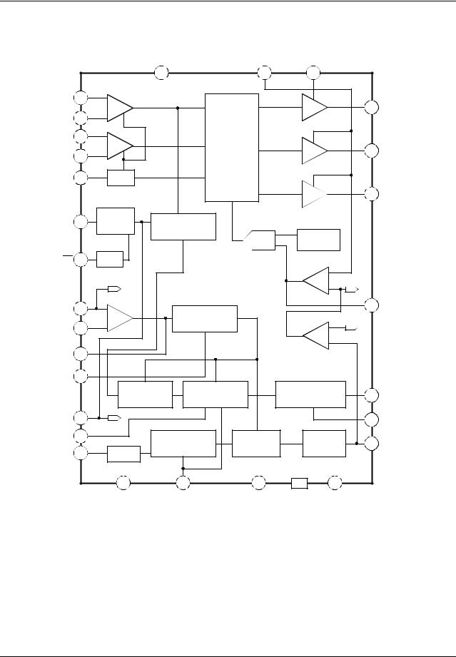
Internal Block Diagram
|
|
VCC |
CURRENT |
CURRENT |
|
|
|
|
|
|
DETECTION2 |
DETECTION1 |
|
|
|||
|
|
16 |
|
17 |
26 |
|
|
|
U INPUT (+) |
19 |
+ |
|
|
|
|
|
|
|
|
U_AMP |
|
|
U_OUT |
|
23 |
U PHASE |
U INPUT(−) |
18 |
− |
|
|
|
|
|
OUTPUT |
|
|
|
|
|
|
|
||
V INPUT (+) |
24 |
+ |
Output |
|
|
|
|
|
|
|
V_AMP |
|
|
|
22 |
|
|
|
|
Control |
|
V_OUT |
|
U PHASE |
||
V INPUT(−) |
25 |
− |
|
|
||||
|
|
|
|
|
|
OUTPUT |
||
AGC |
2 |
AGC |
|
|
|
|
|
|
|
|
|
|
|
W_OUT |
|
21 |
W PHASE |
|
|
|
|
|
|
|
|
OUTPUT |
HALL BIAS |
27 |
Start-up |
Hall |
|
|
|
|
|
|
|
|
Zero-cross |
|
|
|
|
|
|
|
|
|
|
TSD |
|
|
|
CE |
7 |
CE |
|
|
|
|
|
|
|
|
|
|
|
CON_AMP − |
|
|
|
|
|
1.3V |
|
|
+ |
|
|
|
|
|
FG_AMP |
|
|
|
|
0.24V |
|
FG INPUT(+) |
28 |
|
|
|
|
15 |
PHASE |
|
+ |
|
|
|
|
||||
|
|
|
|
|
COMPENSATION |
|||
|
|
|
FG |
|
|
|
|
|
|
|
|
|
|
|
|
|
|
FG INPUT(−) |
1 |
− |
Zero-cross |
|
− |
|
|
|
|
|
|
|
0.69V |
|
|||
|
|
|
|
|
|
|
|
|
|
|
|
|
|
+ |
|
|
|
|
10 |
|
|
BUF_AMP |
|
|
|
|
FG OUTPUT |
|
|
|
|
|
|
|
|
FG ZERO |
9 |
|
|
|
|
|
|
|
CROSS |
|
|
|
|
|
|
|
|
|
|
Timing |
Burst_time |
|
Pulse_width |
|
6 |
INDEX |
|
|
Detectpr |
Circuit |
|
Adjustment |
|
||
|
|
|
|
|
|
|
|
OUTPUT |
VOLTAGE REG. |
4 |
|
|
|
|
|
3 |
INDEX PULSE |
|
|
|
|
|
|
|
||
|
|
2.2V |
|
|
|
|
|
WIDTH |
INDEX BURST |
5 |
|
Rpm_select |
Speed |
Charge |
12 |
|
|
|
|
|
CHARGE |
|||||
|
|
|
11_divider |
Control |
Pump |
|||
OSC INPUT |
13 |
|
|
PUMP |
||||
OSC |
|
|
|
|
|
|||
|
|
|
|
|
OUTPUT |
|||
|
|
|
|
|
|
|
|
|
|
|
14 |
11 |
8 |
|
20 |
|
|
|
|
NC |
RPM |
SIGNAL |
FIN |
NC |
|
|
|
|
|
SELECT |
GROUND |
|
|
|
|
4

KA2822D
Equivalent Circuits
|
U_amp, V_ amp input |
|
U, V, W drive output and current detection 1, 2 |
|||
|
vcc |
|
|
|
|
(17Pin, |
|
|
|
|
|
|
|
|
|
|
|
|
|
26Pin) |
vcc |
|
vcc |
|
|
|
VCC |
|
|
|
|
(16Pin) |
||
|
|
5kΩ |
|
|
|
|
2.5kΩ |
|
2.5kΩ |
|
U |
|
|
|
|
|
|
V |
|
|
(19Pin, |
|
(18Pin, |
|
(23Pin) |
|
|
|
|
(22Pin) |
W |
|||
25Pin) |
|
24Pin) |
|
|
||
|
|
|
|
(21Pin) |
||
|
|
|
40kΩ |
40kΩ |
40kΩ |
|
FG input and FG output |
|
|
OSC input |
|
||
|
vcc |
|
|
|
|
vcc |
vcc |
vcc |
|
|
|
|
|
|
|
|
|
|
||
0.5kΩ |
0.5kΩ |
|
|
vcc |
|
|
|
|
|
|
|
||
|
(28Pin) |
|
0.1kΩ |
|
|
|
|
|
|
|
1kΩ |
|
|
|
vcc |
(13Pin) |
|
|
|
|
|
|
|
50pF |
|
||
25kΩ |
|
vcc |
|
|
|
|
|
|
5kΩ |
|
|
||
|
|
|
|
|
|
|
|
|
(10Pin) |
|
|
|
|
|
CE input |
|
Hall bias input and voltage regulator output |
|||
|
|
|
|
vcc |
vcc |
|
|
vcc |
|
|
vcc |
|
|
|
|
|
|
|
|
|
|
vcc |
|
|
|
|
2.9V |
|
|
(27Pin) |
|
|
vcc |
|
|
|
|
|
|
||
|
|
|
|
|
|
|
CE |
3kΩ |
|
|
|
|
|
|
|
|
|
|
(4Pin) |
|
|
|
|
|
|
2.2V |
|
|
|
|
5 |
|
|
|
 Loading...