


September 1997
Revised April 2000
GTLP8T306
8-Bit LVTTL/GTLP Bus Transceiver
General Description
The GTLP8T306 is an 8-bit bus transceiver that provides LVTTL to GTLP signal level translation. The device provides a high speed interface between cards operating at LVTTL logic levels and a backplane operating at GTLP logic levels. High speed backplane operation is a direct result of GTLP’s reduced output swing (< 1V), reduced input threshold levels and output edge rate control. The edge rate control minimizes bus settling time. GTLP is a Fairchild Semiconductor derivative of the Gunning Transceiver logic (GTL) JEDEC standard JESD8-3.
Fairchild’s GTLP has internal output edge-rate control and is process, voltage, and temperature (PVT) compensated. Its function is similar to BTL and GTL but with different output levels and receiver thresholds. The GTLP output LOW level is typically less than 0.5V, the output HIGH level is 1.5V and the receiver threshold is 1.0V.
Features
■Bidirectional interface between GTL/GTLP and LVTTL logic levels
■Output Edge Rate Control to minimize noise on the GTLP port
■Power up/down/off high impedance for live insertion
■Standard 245 function
■CMOS technology for low power dissipation
■5V tolerant inputs and outputs on the A-Port
■Bus-hold data inputs on the A-Port eliminates the need for external pull-up resistors on unused inputs
■LVTTL compatible driver and control inputs
■Flow through pinout optimizes PCB layout
■Open drain on GTLP to support wired-or connection
■A-Port source/sink − 24 mA/+ 24 mA
■B-Port sink 50 mA
■Recommended Operating Temperature − 40° C to + 85° C
Ordering Code:
Order Number |
Package Number |
Package Description |
|
|
|
GTLP8T306MTC |
MTC24 |
24-Lead Thin Shrink Small Outline Package (TSSOP), JEDEC MO-153, 4.4mm Wide |
|
|
|
Devices also available in Tape and Reel. Specify by appending the suffix letter “X” to the ordering code.
Logic Symbol |
Connection Diagram |
Transceiver Bus LVTTL/GTLP Bit-8 GTLP8T306
© 2000 Fairchild Semiconductor Corporation |
DS500051 |
www.fairchildsemi.com |
GTLP8T306
Pin Descriptions |
Truth Table |
|
|
Pin Names |
Description |
||
|
|
|
|
||
|
|
|
|
|
Output Enable (Active LOW) |
|
OE |
|
|
||
|
|
||||
|
|
|
|
|
Transmit/Receive Input |
T/R |
|
||||
|
|
||||
A0–A7 |
Side A Inputs or 3-STATE Outputs |
||||
|
|
||||
B0–B7 |
Side B Inputs or 3-STATE Outputs |
||||
|
|
|
|||
|
VREF |
GTLP Reference Voltage |
|||
|
|
Inputs |
|
Output |
||
|
|
|
|
|
|
|
OE |
|
T/R |
|
|
||
|
|
|
|
|
|
|
|
H |
|
X |
|
HIGH Z on Bus A and Bus B |
|
|
|
|
|
|
|
|
|
L |
|
L |
|
Bus B Data to Bus A |
|
|
L |
|
H |
|
Bus A Data to Bus B |
|
|
|
|
|
|
|
|
Functional Description
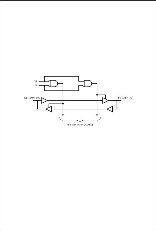
The GTLP8T306 is an 8-bit transceiver providing the standard 245 functionality that supports both GTL and GTLP signal levels.
Data polarity is non-inverting and the data flow direction is controlled by the T/R pin. The outputs are enabled to allow data through the device when OE is LOW otherwise both the A and B ports are placed in a HIGH impedance state.
Logic Diagram
www.fairchildsemi.com |
2 |

Absolute Maximum Ratings(Note 1)
Supply Voltage (VCC) |
− 0.5V to 7.0V |
|
DC Input Voltage (VI) |
− 0.5V to + 7.0V |
|
DC Output Voltage (VO) |
|
|
Outputs 3-STATE |
− 0.5V to + 7.0V |
|
Outputs Active (Note 2) |
− 0.5V to 7.0V |
|
DC Output Sink Current into A-Port |
|
|
IOL |
|
48 mA |
DC Output Source Current from |
|
|
A-Port IOH |
− 48 mA |
|
DC Output Sink Current into B-Port |
|
|
in the LOW State, IOL |
100 mA |
|
DC Input Diode Current (IIK) |
|
|
VI < |
0V |
− 50 mA |
DC Output Diode Current (IOK) |
|
|
VO < |
0V |
− 50 mA |
VO > |
VCC |
+ 50 mA |
ESD Rating |
> 2000V |
|
Storage Temperature (TSTG) |
− 65° C to + 150° C |
|
Recommended Operating
Conditions (Note 3)
Supply Voltage VCC |
3.15V to 3.45V |
Bus Termination Voltage (VTT) |
|
GTLP |
1.35V to 1.65V |
GTL |
1.14V to 1.26V |
Input Voltage (VI) on A-Port |
|
and control pins |
0V to 5.5V |
HIGH Level Output Current (IOH) |
|
A-Port |
− 24 mA |
LOW Level Output Current (IOL) |
|
A-Port |
+ 24 mA |
B-Port |
+ 50 mA |
Operating Temperature (TA) |
− 40° C to + 85° C |
Note 1: The Absolute Maximum Ratings are those values beyond which the safety of the device cannot be guaranteed. The device should not be operated at these limits. The parametric values defined in the Electrical Characteristics tables are not guaranteed at the absolute maximum rating. The “Recommended Operating Conditions” table will define the conditions for actual device operation.
Note 2: IO Absolute Maximum Rating must be observed.
Note 3: Unused inputs must be held high or low.
GTLP8T306
3 |
www.fairchildsemi.com |
 Loading...