


KA79M24
Fairchild Semiconductor KA79M24, KA79M18, KA79M15, KA79M12, KA79M05 Datasheet
...
©2001 Fairchild Semiconductor Corporation
www.fairchildsemi.com
Rev. 1.0.0
Features
• No external components required
• Output current in excess of 0.5A
• Internal thermal overload
• Internal short circuit current limiting
• Output transistor safe area compensation
• Output volt ages of -5V,-6V,-8V, -12V,-15V,-18V,-24V
Description
The KA79MXX series of 3-Terminal medium current
negative voltage regulators are monolithic integrated circuits
designed as fixed voltage regulators. These regulators
employ internal current limiting, thermal shutdown and
safe area compensation making them essentially
indestructible.
TO-220
D-PAK
1. GND 2. Input 3. Output
1
1
Schematic Diagram
KA79MXX
3-Terminal 0.5A Negative V oltage R egulator
KA79MXX
2
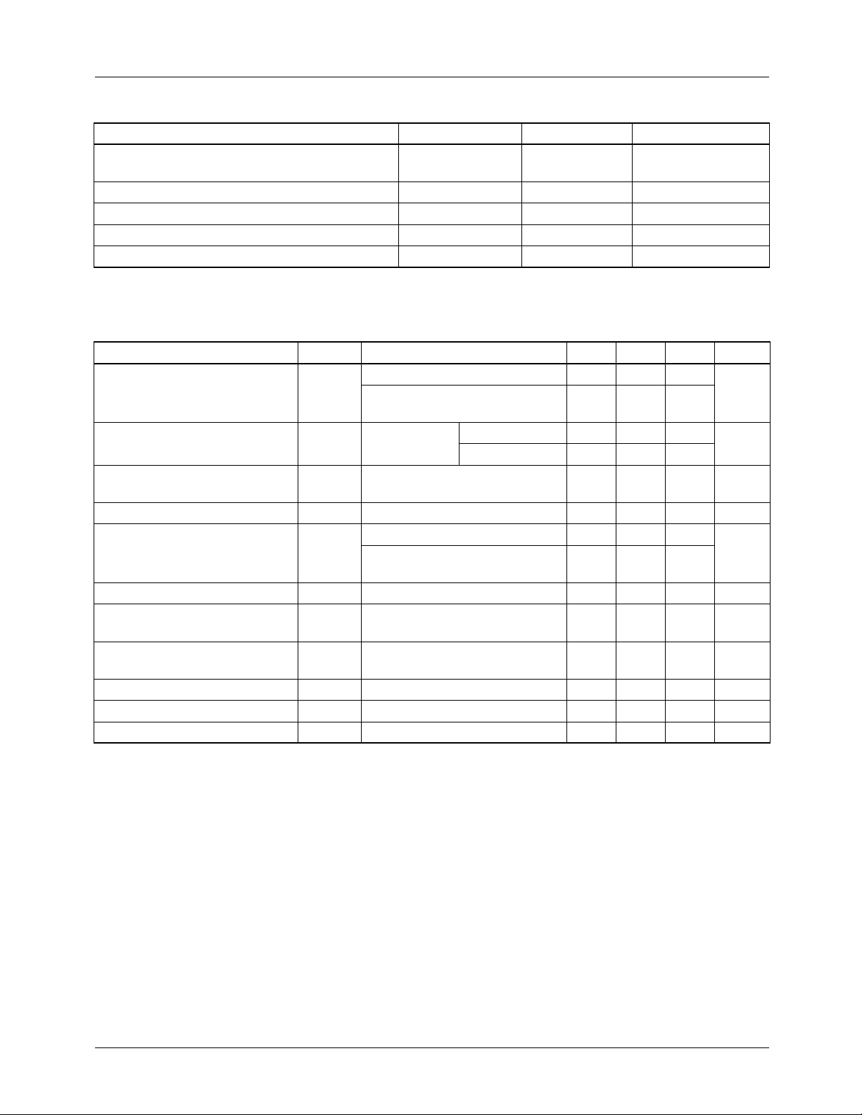
Absolute Maximum Ratings
Electrical Characteristics (KA79M05/KA79M05R)
(Refer to test circuit, 0
°C ≤T
J
≤ +125
°C, l
O
=350mA, V
I
=-10V,unless otherwise specified, C
I
=0.33µF,C
O
=0.1µF)
Note:
1. Load and line regulation are specified at constant junction temperature. Change in V
O
due to heating effects must be taken
into account separately. Pulse testing with low duty is used.
Parameter Symbol Value Unit
Input Voltage(for V
O
= -5V to -18V)
(for V
O
= -24V)
V
I
V
I
-35
-40
V
V
Thermal Resistance Junction-Cases R
θJC
5 °C /W
Thermal Resistance Junction-Air R
θJA
65 °C /W
Operating Temperature Range T
OPR
0 ~ +125 °C
Storage Temperature Range T
STG
-65 ~ +125 °C
Parameter Symbol Conditions Min. Typ. Max. Unit
Output Voltage V
O
T
J
= +25 °C -4.8 -5 -5.2
V
I
O
= 5mA to 350mA
V
I
= -V7 to -25V
-4.75 -5 -5.25
Line Regulation (Note1) ∆V
O
T
J
=+25°C
V
I
= -7V to -25V - 7.0 50
mV
V
I
= -8V to -25V - 2.0 30
Load Regulation (Note1) ∆V
O
I
O
= 5mA to 500mA
T
J
= +25 °C
- 30 100 mV
Quiescent Current I
Q
T
J
= +25 °C-3.06.0mA
Quiescent Current Change ∆I
Q
I
O
= 5mA to 350mA - - 0.4
mA
I
O
= 200mA
V
I
= -8V to -25V
--0.4
Output Voltage Drift ∆Vo/∆TI
O
= 5mA - -0.2 - mV/ °C
Output Noise Voltage V
N
f = 10Hz, 100KHz
T
A
= +25 °C
-40-µV
Ripple Rejection RR
f = 120Hz
V
J
= -8Vto -18V
54 60 - dB
Dropout Voltage V
D
T
J
=+25 °C, I
O
= 500mA - 1.1 - V
Short Circuit Current I
SC
T
J
= +25 °C, V
I
= -35V - 140 - mA
Peak Current I
PK
T
J
= +25 °C - 650 - mA

KA79MXX
3
Electrical Characteristics (KA79M06)
(Refer to test circuit, 0
°C ≤T
J
≤ +125 °C, l
O
=350mA, V
I
= -11V,unless otherwise specified)
Note:
1. Load and line regulation are specified at constant junction temperature. Change in V
O
due to heating effects must be taken
into account separately. Pulse testing with low duty is used.
Parameter Symbol Conditions Min. Typ. Max. Unit
Output Voltage V
O
T
J
= +25 °C - 5.75 - 6.0 - 6.25
V
I
O
= 5mA to 350mA
V
I
= -8.0V to -25V - 5.7 - 6.0 - 6.3
Line Regulation (Note1) ∆V
O
T
J
=+25°C
V
I
= -8Vto -25V - 7.0 60
mV
V
I
= -9V to -19V - 2.0 40
Load Regulation (Note1) ∆V
O
T
J
= +25 °CI
O
= 5.0mA to 500mA - 30 120 mV
Quiescent Current I
Q
T
J
= +25 °C-36mA
Quiescent Current Change ∆I
Q
I
O
= 5mA to 350mA - - 0.4
mA
V
I
= -8V to -25V - - 0.4
Output Voltage Drift ∆V
O
/∆TI
O
= 5mA - 0.4 - mV/ °C
Output Noise Voltage V
N
f = 10Hz to 100KHz,T
A
= +25 °C-50-µV
Ripple Rejection RR f = 120Hz,V
I
= -9V to -19V 54 60 - dB
Dropout Voltage V
D
I
O
= 500mA, T
J
= +25 °C-1.1-V
Short Circuit Current I
SC
V
I
= -35V, T
J
= +25 °C - 140 - mA
Peak Current I
PK
T
J
= +25 °C - 650 - mA

KA79MXX
4
Electrical Characteristics (KA79M08/KA79M08R)
(Refer to test circuit, 0
°C ≤T
J
≤ +125 °C, l
O
=350mA, V
I
= -14V,unless otherwise specified)
Note:
1. Load and line regulation are specified at constant junction temperature. Change in V
O
due to heating effects must be taken
into account separately. Pulse testing with low duty is used.
Parameter Symbol Conditions Min. Typ. Max. Unit
Output Voltage V
O
T
J
= +25 °C - 7.7 - 8.0 - 8.3
V
I
O
= 5mA to 350mA
V
I
= -10.5V to -25V - 7.6 - 8.0 - 8.4
Line Regulation (Note1) ∆V
O
T
J
=+25°C
V
I
= -10.5V to -25V - 7.0 80
mV
V
I
= -11V to -21V - 2.0 50
Load Regulation (Note1) ∆V
O
T
J
= +25 °CI
O
= 5.0mA to 500mA - 30 160 mV
Quiescent Current I
Q
T
J
= +25 °C-36mA
Quiescent Current Change ∆I
Q
I
O
= 5mA to 350mA - - 0.4
mA
V
I
= -8V to -25V - - 0.4
Output Voltage Drift ∆V
O
/∆TI
O
= 5mA - -0.6 - mV/ °C
Output Noise Voltage V
N
f = 10Hz to 100KHz,T
A
= +25 °C-60-µV
Ripple Rejection RR f = 120Hz,V
I
= -9V to -19V 54 59 - dB
Dropout Voltage V
D
I
O
= 500mA, T
J
= +25 °C-1.1-V
Short Circuit Current I
SC
V
I
= -35V, T
J
= +25 °C - 140 - mA
Peak Current I
PK
T
J
= +25 °C - 650 - mA
KA79MXX
5
Electrical Characteristics (KA79M12)
(Refer to test circuit, 0
°C ≤T
J
≤ +125 °C, l
O
=350mA, V
I
= -19V,unless otherwise specified)
Note:
1. Load and line regulation are specified at constant junction temperature. Change in V
O
due to heating effects must be taken
into account separately. Pulse testing with low duty is used.
Parameter Symbol Conditions Min. Typ. Max. Unit
Output Voltage V
O
T
J
= +25 °C -11.5 -12 -12.5
V
I
O
= 5mA to 350mA
V
I
= -14.5V to -30V -11.4 -12 -12.6
Line Regulation (Note1) ∆V
O
T
J
=+25°C
V
I
= -14.5V to -30V - 8.0 80
mV
V
I
= -15V to -25V - 3.0 50
Load Regulation (Note1) ∆V
O
T
J
= +25 °CI
O
= 5.0mA to 500mA - 30 240 mV
Quiescent Current I
Q
T
J
= +25 °C-36mA
Quiescent Current Change ∆I
Q
I
O
= 5mA to 350mA - - 0.4
mA
V
I
= -14.5V to -30V - - 0.4
Output Voltage Drift ∆V
O
/∆TI
O
= 5mA - -0.8 - mV/ °C
Output Noise Voltage V
N
f = 10Hz to 100KHz,T
A
=+25 °C-75-µV
Ripple Rejection RR f = 120Hz,V
I
= -15V to -25V 54 60 - dB
Dropout Voltage V
D
I
O
= 500mA, T
J
= +25 °C-1.1-V
Short Circuit Current I
SC
V
I
= -35V, T
J
= +25 °C - 140 - mA
Peak Current I
PK
T
J
= +25 °C - 650 - mA
 Loading...