Fairchild Semiconductor H21B3, H21B2, H21B1 Datasheet

PHOTODARLINGTON OPTICAL INTERRUPTER SWITCH
H21B1 H21B2 H21B3
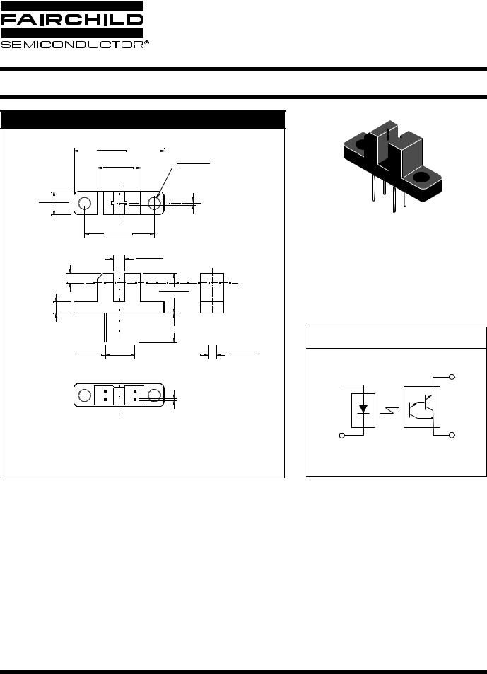
PACKAGE DIMENSIONS
0.972 (24.7) |
|
|
||
|
0.957 (24.3) |
|
|
Ø 0.133 (3.4) |
0.472 (12.0) |
|
|||
|
Ø 0.126 (3.2) |
|||
0.457 (11.6) |
|
|||
|
(2X) |
|||
|
C |
|||
|
|
|||
|
L |
|
||
|
|
|
|
|
0.249 (6.35) |
+ |
D |
|
C |
|
0.243 (6.15) |
|
L |
|
E |
+ |
|
|
0.39 (1.00) |
|
|
0.34 (0.85) |
0.755 (19.2)
0.745 (18.9)
0.129 (3.3)
0.119 (3.0)
0.103 (2.60) NOM |
|
Optical |
|
0.433 (11.0) |
C |
|
L |
|
|
0.422 (10.7) |
|
0.125 (3.2) |
0.315 (8.0) |
|
0.119 (3.0) |
|
|
|
|
|
|
C |
|
.295 (7.5) |
L |
0.110 (2.8) |
|
||
.272 (6.9) |
|
0.091 (2.3) |
|
|
PIN 1 ANODE |
|
|
PIN 2 CATHODE |
2 |
3 |
PIN 3 COLLECTOR |
1 |
4 |
PIN 4 EMITTER |
|
0.020 (0.51) (SQ) |
|
NOTES:
1.Dimensions for all drawings are in inches (mm).
2.Tolerance of ± .010 (.25) on all non-nominal dimensions unless otherwise specified.
SCHEMATIC
4
1
2 |
3 |
DESCRIPTION
The H21B1, H21B2 and H21B3 consist of a gallium arsenide infrared emitting diode coupled with a silicon photodarlington in a plastic housing. The packaging system is designed to optimize the mechanical resolution, coupling efficiency, ambient light rejection, cost and reliability. The gap in the housing provides a means of interrupting the signal with an opaque material, switching the output from an “ON” to an “OFF” state.
FEATURES
•Opaque housing
•Low cost
•.035" apertures
•High IC(ON)
© 2002 Fairchild Semiconductor Corporation |
Page 1 of 6 |
6/13/02 |

PHOTODARLINGTON
OPTICAL INTERRUPTER SWITCH
|
H21B1 |
H21B2 |
H21B3 |
|
|
|
|
|
|
|
|
ABSOLUTE MAXIMUM RATINGS (TA = 25°C unless otherwise specified) |
|
||
|
|
|
|
Parameter |
Symbol |
Rating |
Unit |
|
|
|
|
Operating Temperature |
TOPR |
-55 to +100 |
°C |
Storage Temperature |
TSTG |
-55 to +100 |
°C |
Soldering Temperature (Iron)(2,3 and 4) |
TSOL-I |
240 for 5 sec |
°C |
Soldering Temperature (Flow)(2 and 3) |
TSOL-F |
260 for 10 sec |
°C |
INPUT (EMITTER) |
|
|
|
Continuous Forward Current |
IF |
50 |
mA |
|
|
|
|
Reverse Voltage |
VR |
6 |
V |
Power Dissipation(1) |
PD |
100 |
mW |
OUTPUT (SENSOR) |
|
|
|
Collector to Emitter Voltage |
VCEO |
30 |
V |
Emitter to Collector Voltage |
VECO |
6 |
V |
Collector Current |
IC |
40 |
mA |
Power Dissipation (T = 25°C)(1) |
PD |
150 |
mW |
C |
|
|
|
NOTES:
1.Derate power dissipation linearly 1.67 mW/°C above 25°C.
2.RMA flux is recommended.
3.Methanol or isopropyl alcohols are recommended as cleaning agents.
4.Soldering iron 1/16" (1.6 mm) minimum from housing.
© 2002 Fairchild Semiconductor Corporation |
Page 2 of 6 |
6/13/02 |
 Loading...