


FST16211MTDX
Fairchild Semiconductor FST16211MTDX, FST16211MTD, FST16211MEAX, FST16211MEA, FST16211GX Datasheet
...
© 2000 Fairchild Semiconductor Corporation DS500037 www.fairchildsemi.com
July 1997
Revised August 2000
FST16211 24-Bit Bus Switch
FST16211
24-Bit Bus Switch
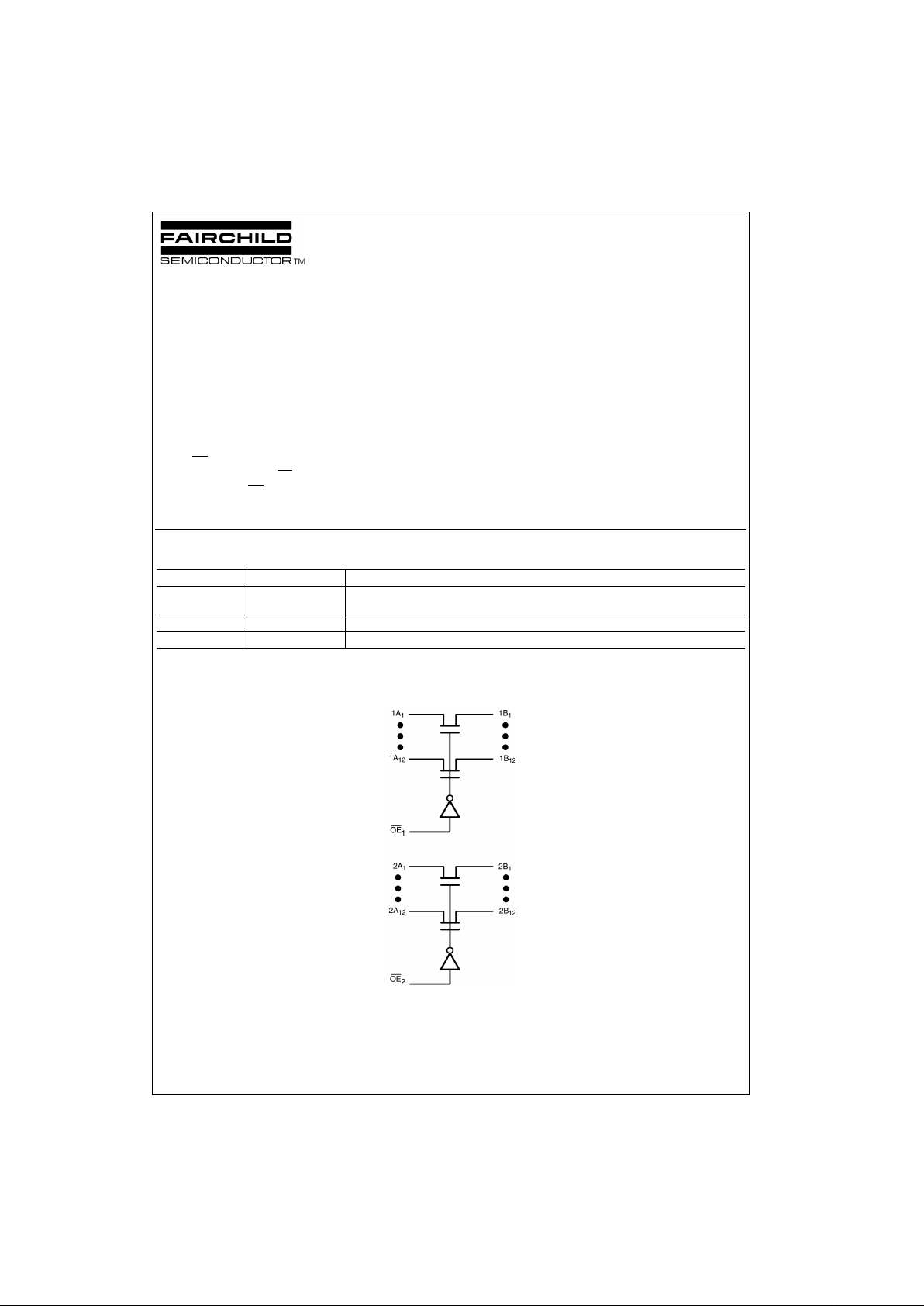
General Description
The Fairchild Sw itch FST16211 provides 24-bits of highspeed CMOS TTL-comp atible bus switching. The low on
resistance of the switch allows inp uts to be connected to
outputs without adding propagation delay or generating
additional ground bounce noise.
The device is organi zed as a 12-bit or 24-bit b us switch.
When OE
1
is LOW, the switch is ON and Port 1A is con-
nected to Port 1B. When OE
2
is LOW, Port 2A is connected
to Port 2B. When OE
1/2
is HIGH, a high impedance state
exists between the A and B Ports.
Features
■ 4Ω switch connection between two ports
■ Minimal propagation delay through the switch
■ Low l
CC
■ Zero bounce in flow-through mode
■ Control inputs compatible with TTL level
■ Also packaged in plastic Fine Pitch Ball Grid Array
(FBGA)
Ordering Code:
Devices also availab le in Tape and Reel. Specify by appending th e s uffix let t er “X” to the ordering code.
Note 1: BGA package available in Tape and Reel only.
Logic Diagram
Order Number Package Number Package Description
FST16211GX
(Note 1)
BGA54A
Preliminary
54-Ball Fine-Pitch Ball Grid Array (FBGA), JEDEC MO-195, 5.5mm Wide
[TAPE and REEL]
FST16211MEA MS56A 56-Lead Shrink Small Outline Package (SSOP), JEDEC MO-118, 0.300 Wide
FST16211MTD MTD56 56-Lead Thin Shrink Small Outline Package (TSSOP), JEDEC MO-153, 6.1mm Wide
www.fairchildsemi.com 2
FST16211
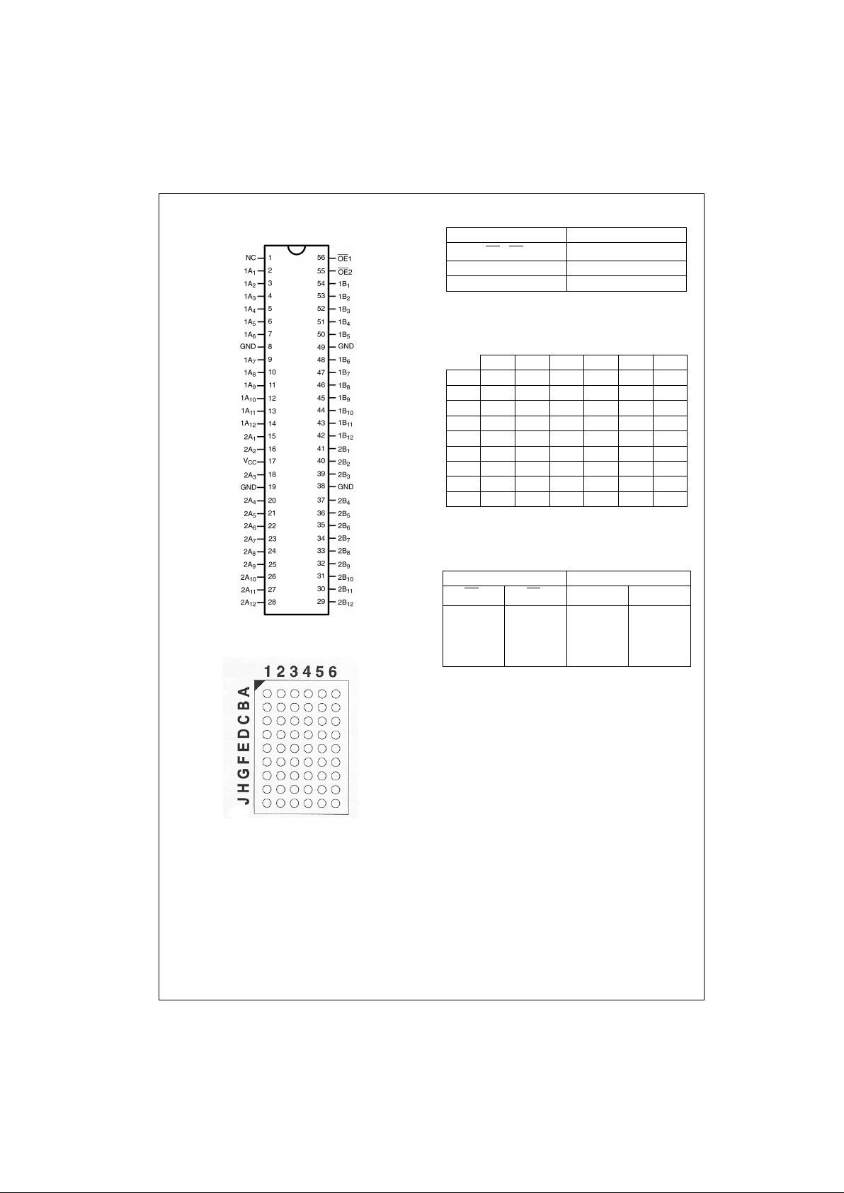
Connection Diagrams
Pin Assignment fo r SSOP and TSSOP
Pin Assignment for FBGA
TOP VIEW
Pin Descriptions
FBGA Pin Assignments
Tr uth Table
Pin Name Description
OE
1
, OE
2
Bus Switch Enables
1A, 2A Bus A
1B, 2B Bus B
123456
A 1A
2
1A1NC OE21B11B
2
B 1A41A31A7OE11B31B
4
C 1A61A5GND 1B71B51B
6
D 1A101A91A81B81B91B
10
E 1A121A112A12B11B111B
12
F 2A42A32A22B22B32B
4
G 2A62A5VCCGND 2B52B
6
H 2A82A72A112B112B72B
8
J 2A102A92A122B122B92B
10
Inputs Inputs/Outputs
OE
1
OE
2
1A, 1B 2A, 2B
LL1A
= 1B 2A = 2B
LH1A
= 1B Z
HLZ2A
= 2B
HHZZ
3 www.fairchildsemi.com
FST16211
Absolute Maximum Ratings(Note 2) Recommended Operating
Conditions
(Note 5)
Note 2: The “Absolute Maximum Ratings” are those value s beyond which
the safety of the dev ice cannot b e guaranteed . The device sh ould not be
operated at these limit s. The parametric values defi ned in the Electrical
Characteristics tables are not guaranteed at the absolute maximum rating.
The “Recomm ended O peratin g Cond itions ” table will defin e the condition s
for actual device operation.
Note 3: V
S
is the voltage observed/applied at either A or B Ports across the
switch.
Note 4: The input and output negative voltage ratings may be exceeded if
the input and ou t put diode current ratings are observed.
Note 5: Unused control inputs must be held HIGH or LOW. They may not
float.
DC Electrical Characteristics
Note 6: Typical values are at VCC = 5.0V and TA = +25°C
Note 7: Measured by the voltage drop between A and B pins at the indicated current through the switch. On resistance is determined by the lower of the
voltages on the two (A or B) pins.
Supply Voltage (VCC) −0.5V to +7.0V
DC Switch Voltage (V
S
) (Note 3) −0.5V to +7.0V
DC Input Voltage (V
IN
) (Note 4) −0.5V to +7.0V
DC Input Diode Current (l
IK
) V
IN
<0V −50mA
DC Output (I
OUT
) Sink Current 128mA
DC V
CC
/GND Current (ICC/I
GND
) +/− 100mA
Storage Temperature Range (T
STG
) −65°C to +150 °C
Power Supply Operating (V
CC)
4.0V to 5.5V
Input Voltage (V
IN
) 0V to 5.5V
Output Voltage (V
OUT
) 0V to 5.5V
Input Rise and Fall Time (t
r
, tf)
Switch Control Input 0nS/V to 5nS/V
Switch I/O 0nS/V to DC
Free Air Operating Temperature (T
A
)-40 °C to +85 °C
Symbol Parameter
V
CC
(V)
TA = −40 °C to +85 °C
Units Conditions
Min T yp
(Note 6)
Max
V
IK
Clamp Diode Voltage 4.5 −1.2 V IIN = −18mA
V
IH
HIGH Level Input Voltage 4.0–5.5 2.0 V
V
IL
LOW Level Input Voltage 4.0–5.5 0.8 V
I
I
Input Leakage Current 5.5 ±1.0 µA0 ≤ VIN ≤ 5.5V
010µAV
IN
= 5.5V
I
OZ
OFF-STATE Leakage Current 5.5 ±1.0 µA0 ≤ A, B ≤ V
CC
R
ON
Switch On Resistance 4.5 4 7 Ω VIN = 0V, IIN = 64mA
(Note 7) 4.5 4 7 Ω V
IN
= 0V, IIN = 30mA
4.5 8 12 Ω V
IN
= 2.4V, IIN = 15mA
4.0 11 20 Ω VIN = 2.4V, IIN = 15mA
I
CC
Quiescent Supply Current 5.5 3 µAVIN = VCC or GND, I
OUT
= 0
∆ I
CC
Increase in I
CC
per Input 5.5 2.5 mA One input at 3.4V
Other inputs at VCC or GND
 Loading...