Fairchild Semiconductor GTLP16612MTDX, GTLP16612MTD, GTLP16612MEAX, GTLP16612MEA Datasheet

March 1995
Revised October 1998
GTLP16612
CMOS 18-Bit TTL/GTLP Universal Bus Transceiver
General Description
The GTLP16612 is an 18-bit universal bus transceiver which provides TTL to GTLP signal level translation. The device is designed to provide a high speed interface between cards operating at TTL logic levels and a backplane operating at GTLP logic levels. High speed backplane operation is a direct result of GTLP’s reduced output swing (<1V), reduced input threshold levels and output edge rate control which minimizes signal settling times. GTLP is a Fairchild Semiconductor derivative of the Gunning Transceiver Logic (GTL) JEDEC standard JESD8-3.
Fairchild’s GTLP has internal edge-rate control and is Process, Voltage, and Temperature (PVT) compensated. Its function is similar to BTL or GTL but with different driver output levels and receiver threshold. GTLP output low voltage is typically less than 0.5V, the output high is 1.5V and the receiver threshold is 1.0V.
Features
■Bidirectional interface between GTLP and TTL logic levels
■Designed with Edge Rate Control Circuit to reduce output noise
■VREF pin provides external supply reference voltage for receiver threshold
■Submicron Core CMOS technology for low power dissipation
■Special PVT Compensation circuitry to provide consistent performance over variations of process, supply voltage and temperature
■5V tolerant inputs and outputs on A-Port
■Bus-Hold data inputs on A-Port to eliminate the need for external pull-up resistors for unused inputs
■Power up/down high impedance
■TTL compatible Driver and Control inputs
■ A-Port outputs source/sink −32 mA/+32 mA
■Flow-through architecture optimizes PCB layout
■Open drain on GTLP to support wired-or connection
Ordering Code:
Order Number |
Package Number |
Package Description |
|
|
|
GTLP16612MEA |
MS56A |
56-Lead Shrink Small Outline Package (SSOP), JEDEC MO-118 0.300” Wide |
|
|
|
GTLP16612MTD |
MTD56 |
56-Lead Thin Shrink Small Outline Package (TSSOP), JEDEC MO-153, 6.1mm Wide |
|
|
|
Device also available in Tape and Reel. Specify by appending suffix letter “X” to the ordering code.
Transceiver Bus Universal TTL/GTLP Bit-18 CMOS GTLP16612
© 1998 Fairchild Semiconductor Corporation |
DS012390.prf |
www.fairchildsemi.com |

GTLP16612
Pin Descriptions |
Connection Diagram |
||||||
|
|
|
|
|
|
||
|
|
|
Pin |
Description |
|
||
|
|
|
Names |
|
|
||
|
|
|
|
|
|
||
|
|
|
|
|
|
A-to-B Output Enable (Active LOW) |
|
|
|
|
OEAB |
|
|
||
|
|
|
|
B-to-A Output Enable (Active LOW) |
|
||
|
|
OEBA |
|
|
|||
|
|
|
A-to-B Clock Enable (Active LOW) |
|
|||
|
|
CEAB |
|
|
|||
|
|
|
B-to-A Clock Enable (Active LOW) |
|
|||
|
|
CEBA |
|
|
|||
|
|
LEAB |
A-to-B Latch Enable (Transparent HIGH) |
|
|||
|
|
LEBA |
B-to-A Latch Enable (Transparent HIGH) |
|
|||
|
|
CLKAB |
A-to-B Clock Pulse |
|
|||
|
|
CLKBA |
B-to-A Clock Pulse |
|
|||
|
|
VREF |
GTLP Input Reference Voltage |
|
|||
|
|
A1–A18 |
A-to-B TTL Data Inputs or |
|
|||
|
|
|
|
|
|
B-to-A 3-STATE Outputs |
|
|
|
B1–B18 |
B-to-A GTLP Data Inputs or |
|
|||
|
|
|
|
|
|
A-to-B Open Drain Outputs |
|
|
|
|
|
|
|
|
|
Functional Description
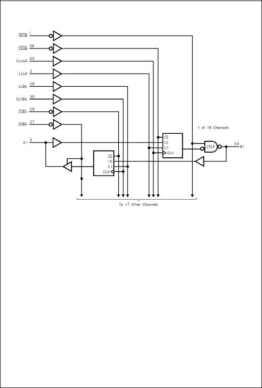
The GTLP16612 combines a universal transceiver function with a TTL to GTLP translation. The A-Port and control pins operate at LVTTL or 5V TTL levels while the B-Port operates at GTLP levels. The transceiver logic includes D-type latches and D-type flip-flops to allow data flow in transparent, latched and clock mode.
The functional operation is described in the truth table below.
Truth Table
(Note 1)
|
|
|
|
Inputs |
|
|
Output |
Mode |
|
|
|
|
|
|
|
B |
|
|
|
|
|
|
|
|
|
|
CEAB |
|
OEAB |
LEAB |
CLKAB |
A |
|
||
|
|
|
||||||
|
|
|
|
|
|
|
|
|
|
X |
|
H |
X |
X |
X |
Z |
Latched |
|
L |
|
L |
L |
H |
X |
B0(Note 2) |
storage |
|
L |
|
L |
L |
L |
X |
B0(Note 3) |
of A data |
|
|
|
|
|
|
|
|
|
|
X |
|
L |
H |
X |
L |
L |
Transparent |
|
X |
|
L |
H |
X |
H |
H |
|
|
|
|
|
|
|
|
|
|
|
L |
|
L |
L |
− |
L |
L |
Clocked storage |
|
L |
|
L |
L |
− |
H |
H |
of A data |
|
|
|
|
|
|
|
|
|
|
H |
|
L |
L |
X |
X |
B0(Note 3) |
Clock inhibit |
|
|
|
|
|
|
|
|
|
Note 1: A-to-B data flow is shown. B-to-A data flow is similar but uses OEBA, LEBA, CLKBA, and CEBA.
Note 2: Output level before the indicated steady-state input conditions were established, provided that CLKAB was high before LEAB went low.
Note 3: Output level before the indicated steady-state input conditions were established.
www.fairchildsemi.com |
2 |

Logic Diagram
GTLP16612
3 |
www.fairchildsemi.com |
 Loading...