


FST16292MEA
© 1999 Fairchild Semiconductor Corporation DS500104 www.fairchildsemi.com
July 1997
Revised December 1999
FST16292 12-Bit to 24-Bit Multiplexer/Demultiplexer Bus Switch
FST16292
12-Bit to 24-Bit Multiplexer/Demultiplexer Bus Switch
General Description
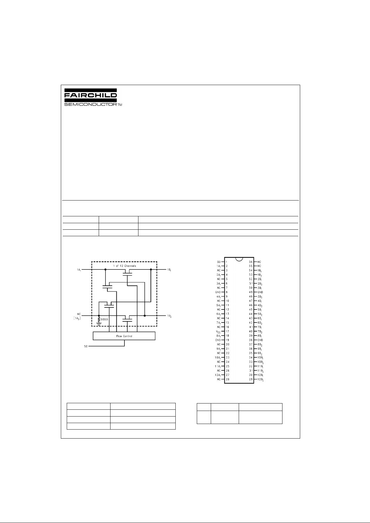
The Fairchild Switch FST16 292 provides twelve 2:1 highspeed CMOS TTL-compatible multiplexer/demultiplexer
bus switches. The low on resistance of the switch allows
inputs to be connect ed to output s with out adding prop agation delay or generating additional ground bounce noise.
The select pin connects the A Port to the selected B Port
output. The A
2
Ports are not externally connected, thus
have a 500Ω pull-down resistor to ground.
Features
■ 4Ω switch connection between two ports.
■ Minimal propagation delay through the switch.
■ Low l
CC
.
■ Zero bounce in flow-through mode.
■ Control inputs compatible with TTL level.
■ Internal 500Ω pull-down resistor on A
2
port.
Ordering Code:
Devices also availab le in Tape and Reel. Specify by appending th e s uffix let t er “X” to the ordering code.
Logic Diagram
Pin Descriptions
Connection Diagram
Truth Table
Order Number Package Number Package Description
FST16292MEA MS56A 56-Lead Shrink Small Outline Package (SSOP), JEDEC MO-118, 0.300 Wide
FST16292MTD MTD56 56-Lead Thin Shrink Small Outline Package (TSSOP), JEDEC MO-153, 6.1mm Wide
Pin Name Description
SO Data-select input
A
1
Bus A
B
1
, B
2
Bus B
S0 A1A
2
Function
LB
1B2
A1 = B1, A2 = B
2
HB2B
1
A1 = B2, A2 = B
1
www.fairchildsemi.com 2
FST16292
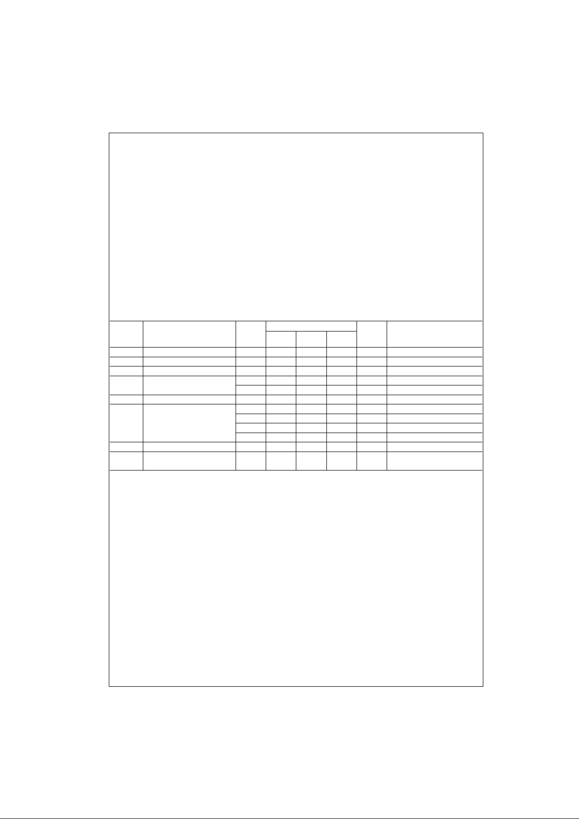
Absolute Maximum Ratings(Note 1) Recommended Operating
Conditions
Note 1: The “Absolute Maximum Ratings” are those values beyon d which
the safety of the dev ice cannot be guaranteed. T he device sh ould not be
operated at these limit s. The parametric values defin ed in the Electrical
Characteristics tables are not guaranteed at the absolute maximum rating.
The “Recomme nded O peratin g Cond itions ” table will defin e the condition s
for actual device operation.
Note 2: The input and output ne gative vo ltage ra tings may be excee ded if
the input and output diode current ratings are observed.
DC Electrical Characteristics
Note 3: Typi c al values are at VCC = 5.0V and TA =+25°C
Note 4: Measured by the volta ge drop between A and B pi ns at th e indicated current through the switch. On resistance is determined by the lower of the
voltages on the two (A or B) pins.
Supply Voltage (VCC) −0.5V to +7.0V
DC Switch Voltage (V
S
) −0.5V to +7.0V
DC Input Voltage (V
IN
) (Note 2) −0.5V to +7.0V
DC Input Diode Current (l
IK
) VIN<0V −50mA
DC Output (I
OUT
) Sink Current 128mA
DC V
CC
/GND Current (ICC/I
GND
) +/− 100mA
Storage Temperature Range (T
STG
) −65°C to +150 °C
Power Supply Operating (V
CC)
4.0V to 5.5V
Input Voltage (V
IN
)0V to 5.5V
Output Voltage (V
OUT
)0V to 5.5V
Input Rise and Fall Time (t
r
, tf)
Switch Control Input 0ns/V to 5ns/V
Switch I/O 0ns/V to DC
Free Air Operating Temperature (T
A
) −40 °C to +85 °C
Symbol Parameter
V
CC
(V)
TA = −40 °C to +85 °C
Units Conditions
Min
Typ
(Note 3)
Max
V
IK
Clamp Diode Voltage 4.5 −1.2 V IIN = −18mA
V
IH
HIGH Level Input Voltage 4.0–5.5 2.0 V
V
IL
LOW Level Input Voltage 4.0–5.5 0.8 V
I
I
Input Leakage Current 5.5 ±1.0 µA0≤ VIN ≤5.5V
010µAVIN = 5.5V
I
OZ
OFF-STATE Leakage Current 5.5 ±1.0 µA0 ≤A, B ≤V
CC
R
ON
Switch On Resistance 4.5 4 7 Ω VIN = 0V, IIN = 64mA
(Note 4) 4.5 4 7 Ω VIN = 0V, IIN = 30mA
4.5 8 12 Ω VIN = 2.4V, IIN = 15mA
4.0 14 20 Ω VIN = 2.4V, IIN = 15mA
I
CC
Quiescent Supply Current 5.5 3 µAVIN = VCC or GND, I
OUT
= 0
∆ I
CC
Increase in I
CC
per Input 5.5 2.5 mA One input at 3.4V
Other inputs at VCC or GND
 Loading...