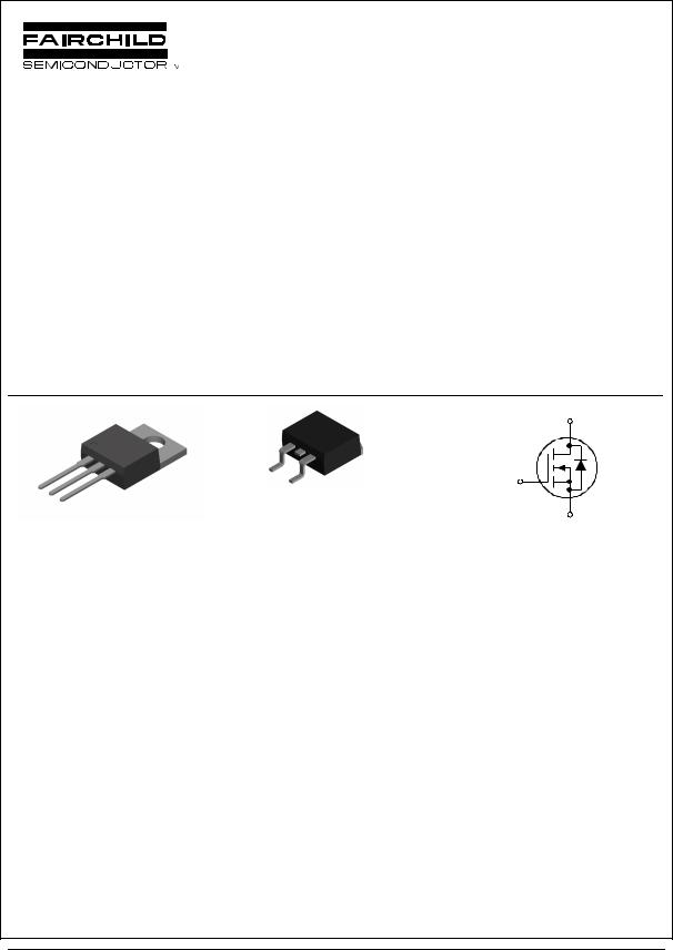
Fairchild Semiconductor FDP7042L, FDB7042L Datasheet

June 2000
PRELIMINARY
FDP7042L / FDB7042L
N-Channel Logic Level PowerTrench MOSFET
General Description
This N-Channel MOSFET has been designed specifically to improve the overall efficiency of DC/DC converters using either synchronous or conventional switching PWM controllers. It has been optimized for “low side” synchronous rectifier operation, providing an extremely low RDS(ON) .
Applications
•Synchronous rectifier
•DC/DC converter
Features
• 50 A, 30 V. RDS(ON) = 9 mΩ @ VGS = 4.5 V RDS(ON) = 7.5 mΩ @ VGS = 10 V
•Critical DC electrical parameters specified at elevated temperature
•High performance trench technology for extremely
low RDS(ON)
•175°C maximum junction temperature rating
|
|
|
D |
|
D |
||
G |
G |
S |
|
|
G |
|
|
TO-220 |
TO-263AB |
|
|
|
|||
D S |
FDP Series |
|
FDB Series |
|
S |
||
|
|
|
|
|
|
||
Absolute Maximum Ratings |
TA=25oC unless otherwise noted |
|
|
|
|||
Symbol |
Parameter |
|
|
Ratings |
|
Units |
|
VDSS |
Drain-Source Voltage |
|
|
|
30 |
|
V |
VGSS |
Gate-Source Voltage |
|
|
|
± 12 |
|
V |
ID |
Drain Current – Continuous |
|
(Note 1) |
|
50 |
|
A |
|
– Pulsed |
|
(Note 1) |
|
150 |
|
|
PD |
Total Power Dissipation @ TC = 25°C |
|
|
83 |
|
W |
|
|
Derate above 25°C |
|
0.48 |
|
W°C |
||
TJ, TSTG |
Operating and Storage Junction Temperature Range |
|
-65 to +175 |
|
°C |
||
Thermal Characteristics |
|
|
|
|
|
|
|
RθJC |
Thermal Resistance, Junction-to-Case |
|
|
1.8 |
|
°C/W |
|
RθJA |
Thermal Resistance, Junction-to-Ambient |
|
|
62.5 |
|
°C/W |
|
Package Marking and Ordering Information
Device Marking |
Device |
Reel Size |
Tape width |
Quantity |
FDB7042L |
FDB7042L |
13’’ |
24mm |
800 units |
FDP7042L |
FDP7042L |
Tube |
n/a |
45 |
FDB7042L / FDP7042L
2000 Fairchild Semiconductor Corporation |
FDP7042L Rev B(W) |

Electrical Characteristics |
|
TA = 25°C unless otherwise noted |
|
|
|
|
|||
Symbol |
Parameter |
|
Test Conditions |
Min |
Typ |
Max |
Units |
||
|
|
|
|
|
|
|
|
|
|
Off Characteristics |
|
|
|
|
|
|
|
|
|
BVDSS |
Drain–Source Breakdown Voltage |
|
VGS = 0 V, ID = 250 µA |
30 |
|
|
V |
||
∆BVDSS |
Breakdown Voltage Temperature |
|
ID = 250 µA, Referenced to 25°C |
|
24 |
|
mV/°C |
||
∆TJ |
Coefficient |
|
|
|
|||||
|
|
|
|
|
|
|
|
||
IDSS |
Zero Gate Voltage Drain Current |
|
VDS = 24 V, |
|
VGS = 0 V |
|
|
1 |
µA |
IGSSF |
Gate–Body Leakage, Forward |
|
VGS = 12 V, |
|
VDS = 0 V |
|
|
100 |
nA |
IGSSR |
Gate–Body Leakage, Reverse |
|
VGS = –12 V |
VDS = 0 V |
|
|
–100 |
nA |
|
On Characteristics (Note 2) |
|
|
|
|
|
|
|
|
|
VGS(th) |
Gate Threshold Voltage |
|
VDS = VGS, ID = 250 µA |
0.8 |
1.2 |
2 |
V |
||
∆VGS(th) |
Gate Threshold Voltage |
|
ID = 250 µA, Referenced to 25°C |
|
–4.1 |
|
mV/°C |
||
∆TJ |
Temperature Coefficient |
|
|
|
|
|
|
||
|
|
|
|
|
|
|
|
||
RDS(on) |
Static Drain–Source On–Resistance |
|
VGS = 4.5 V, |
ID = 25A |
|
6.2 |
9 |
|
|
|
|
|
VGS = 10 V, |
|
ID = 25A |
|
5.5 |
7.5 |
mΩ |
|
|
|
VGS= 4.5 V, ID =25A, TJ=125°C |
|
9.6 |
16 |
|
||
ID(on) |
On–State Drain Current |
|
VGS = 4.5 V, |
VDS = 10 V |
60 |
|
|
A |
|
gFS |
Forward Transconductance |
|
VDS = 5V, |
|
ID = 25 A |
|
117 |
|
S |
Dynamic Characteristics |
|
|
|
|
|
|
|
|
|
Ciss |
Input Capacitance |
VDS = 15 V, |
V GS = 0 V, |
|
2418 |
|
pF |
||
Coss |
Output Capacitance |
|
549 |
|
pF |
||||
f = 1.0 MHz |
|
|
|
|
|||||
Crss |
Reverse Transfer Capacitance |
|
|
|
243 |
|
pF |
||
|
|
|
|
|
|
||||
Switching Characteristics (Note 2) |
|
|
|
|
|
|
|
|
|
td(on) |
Turn–On Delay Time |
|
|
|
|
|
21 |
34 |
ns |
tr |
Turn–On Rise Time |
VDD = 15 V, |
|
ID = 1 A, |
|
20 |
32 |
ns |
|
td(off) |
Turn–Off Delay Time |
VGS = 4.5 V, |
|
RGEN = 6 Ω |
|
60 |
96 |
ns |
|
tf |
Turn–Off Fall Time |
|
|
|
|
|
30 |
48 |
ns |
Qg |
Total Gate Charge |
VDS = 15 V, |
ID = 50 A, |
|
32 |
51 |
nC |
||
Qgs |
Gate–Source Charge |
|
10 |
|
nC |
||||
VGS = 4.5 V |
|
|
|
|
|||||
Qgd |
Gate–Drain Charge |
|
|
|
9 |
|
nC |
||
|
|
|
|
|
|
||||
Drain–Source Diode Characteristics and Maximum Ratings |
|
|
|
|
|||||
IS |
Maximum Continuous Drain–Source Diode Forward Current |
|
|
50 |
A |
||||
VSD |
Drain–Source Diode Forward |
|
VGS = 0 V, |
|
IS = 25 A (Note 2) |
|
0.8 |
1.3 |
V |
Voltage |
|
|
|
||||||
|
|
|
|
|
|
|
|
|
|
Notes:
1.Maximum continuous current is limited by the package.
2.Pulse Test: Pulse Width < 300 s, Duty Cycle < 2.0%
FDB7042L / FDP7042L
FDP7042L Rev B(W)

Typical Characteristics
150 |
VGS = 4.5V |
|
|
|
|
|
|
|
|
|
|
120 |
4.0V |
3.5V |
|
|
|
|
|
|
|
|
|
90 |
|
|
3.0V |
|
|
|
|
|
|
|
|
60 |
|
|
|
|
|
|
|
|
|
2.5V |
|
30 |
|
|
|
|
|
0 |
|
|
|
|
|
0 |
1 |
2 |
3 |
4 |
5 |
VDS, DRAIN-SOURCE VOLTAGE (V)
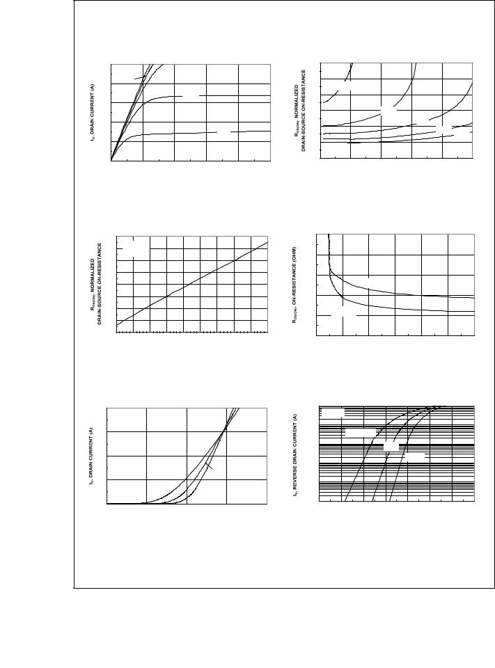
Figure 1. On-Region Characteristics.
2 |
|
|
|
|
|
|
|
|
|
1.8 |
ID =25A |
|
|
|
|
|
|
|
|
VGS = 4.5V |
|
|
|
|
|
|
|
|
|
|
|
|
|
|
|
|
|
|
|
1.6 |
|
|
|
|
|
|
|
|
|
1.4 |
|
|
|
|
|
|
|
|
|
1.2 |
|
|
|
|
|
|
|
|
|
1 |
|
|
|
|
|
|
|
|
|
0.8 |
|
|
|
|
|
|
|
|
|
0.6 |
|
|
|
|
|
|
|
|
|
0.4 |
|
|
|
|
|
|
|
|
|
-50 |
-25 |
0 |
25 |
50 |
75 |
100 |
125 |
150 |
175 |
|
|
TJ, JUNCTION TEMPERATURE (oC) |
|
|
|||||
Figure 3. On-Resistance Variation
withTemperature.
80 |
|
|
|
|
|
VDS = 5V |
|
|
|
60 |
|
|
|
|
40 |
|
|
|
|
|
|
TA = 125oC |
o |
|
20 |
|
|
25 C |
|
|
|
|
|
|
|
|
|
-55oC |
|
0 |
|
|
|
|
1 |
1.5 |
2 |
2.5 |
3 |
VGS, GATE TO SOURCE VOLTAGE (V)
Figure 5. Transfer Characteristics.
2 |
|
|
|
|
|
FDP7042L |
|
|
|
|
|
|
/ |
1.8 |
VGS = 2.5V |
|
|
|
|
FDB7042L |
|
|
|
|
|
||
1.6 |
|
|
|
|
|
|
1.4 |
|
3.0V |
|
|
|
|
1.2 |
|
|
3.5V |
|
|
|
|
|
|
4.0V |
|
|
|
|
|
|
|
4.5V |
|
|
|
|
|
|
|
|
|
1 |
|
|
|
|
|
|
0.8 |
|
|
|
|
|
|
0 |
30 |
60 |
90 |
120 |
|
150 |
|
|
ID, DRAIN CURRENT (A) |
|
|
|
|
Figure 2. On-Resistance Variation with
Drain Current and Gate Voltage.
0.025 |
|
|
|
|
|
|
|
|
|
|
|
ID = 25 A |
|
0.02 |
|
|
|
|
|
|
0.015 |
|
|
|
|
|
|
|
|
TA = 125oC |
|
|
|
|
0.01 |
|
|
|
|
|
|
0.005 |
TA = 25oC |
|
|
|
|
|
|
|
|
|
|
|
|
0 |
|
|
|
|
|
|
2 |
2.5 |
3 |
3.5 |
4 |
4.5 |
5 |
VGS, GATE TO SOURCE VOLTAGE (V)
Figure 4. On-Resistance Variation with
Gate-to-Source Voltage.
100 |
VGS = 0V |
|
|
|
|
|
|
|
|
|
|
|
|
|
|
10 |
|
|
|
|
|
|
|
|
|
TA = 125oC |
|
|
|
|
|
1 |
|
|
25oC |
|
|
|
|
0.1 |
|
|
|
-55oC |
|
|
|
|
|
|
|
|
|
|
|
0.01 |
|
|
|
|
|
|
|
0.001 |
|
|
|
|
|
|
|
0 |
0.2 |
0.4 |
0.6 |
0.8 |
1 |
1.2 |
1.4 |
|
VSD, BODY DIODE FORWARD VOLTAGE (V) |
|
|||||
Figure 6. Body Diode Forward Voltage Variation with Source Current and Temperature.
FDP7042L Rev B(W)
 Loading...