


September 2002
FDD2572 / FDU2572
N-Channel PowerTrench® MOSFET 150V, 29A, 54mΩ
Features |
|
|
|
|
|
|
|
|
|
|
|
|
|
|
|
Applications |
|
|
|
|
|||
• |
rDS(ON) = 45mΩ (Typ.), VGS = 10V, ID = 9A |
|
|
|
|
|
|
|
• DC/DC converters and Off-Line UPS |
|
|
||||||||||||
• Qg(tot) = 26nC (Typ.), VGS = 10V |
|
|
|
|
|
|
|
|
|
• Distributed Power Architectures and VRMs |
|
|
|||||||||||
• |
Low Miller Charge |
|
|
|
|
|
|
|
|
|
|
|
• Primary Switch for 24V and 48V Systems |
|
|
||||||||
|
|
|
|
|
|
|
|
|
|
|
|
|
|
|
|
|
|
|
|
||||
• Low QRR Body Diode |
|
|
|
|
|
|
|
|
|
|
|
• High Voltage Synchronous Rectifier |
|
|
|||||||||
• UIS Capability (Single Pulse and Repetitive Pulse) |
|
|
|
|
|
|
|
||||||||||||||||
|
|
|
|
|
|
|
|
|
|
|
|||||||||||||
• Qualified to AEC Q101 |
|
|
|
|
|
|
|
|
|
|
|
• Direct Injection / Diesel Injection Systems |
|
|
|||||||||
|
|
|
|
|
|
|
|
|
|
|
|
|
|
|
|
|
|||||||
Formerly developmental type 82860 |
|
|
|
|
|
|
|
|
|
|
• 42V Automotive Load Control |
|
|
||||||||||
|
|
|
|
|
|
|
|
|
|
|
|
|
|
|
|
|
|
• Electronic Valve Train Systems |
|
|
|||
|
|
|
|
|
|
|
|
|
|
|
|
|
|
|
|
|
|
|
|
|
|
||
|
|
|
|
|
|
|
|
|
|
|
|
|
|
|
|
|
|
|
|
|
|||
|
|
|
|
|
DRAIN |
|
|
|
|
|
|
|
|
|
SOURCE |
|
|
D |
|
||||
|
|
|
(FLANGE) |
|
|
|
|
|
|
|
|
|
|
|
|
|
|||||||
|
|
|
|
|
|
DRAIN |
|
|
DRAIN |
|
|
|
|
||||||||||
|
|
|
|
|
|
|
|
|
|
|
|
|
|
|
|
|
|
||||||
|
|
|
|
|
|
|
|
|
|
|
|
|
|
GATE |
|
|
|
|
|||||
|
|
|
|
|
|
|
|
|
|
|
|
|
|
|
|
||||||||
|
GATE |
|
|
|
|
|
|
|
|
|
|
(FLANGE) |
|
|
|
|
|
|
|
||||
|
SOURCE |
|
|
|
|
|
|
|
|
|
|
|
|
|
|
|
|
|
|
|
G |
|
|
|
|
|
|
|
|
|
|
|
|
|
|
|
|
|
|
|
|
|
|
|
|
||
|
|
|
|
|
|
|
|
|
|
|
|
|
|
|
|
|
|
|
|
|
|
||
|
|
|
TO-252AA |
|
|
|
|
|
|
|
|
|
|
|
TO-251AA |
|
|
|
|
||||
|
|
|
FDD SERIES |
|
|
|
|
|
|
|
|
|
|
|
|
|
|
|
|||||
|
|
|
|
|
|
|
|
|
|
|
|
|
|
FDU SERIES |
|
|
S |
|
|||||
|
|
|
|
|
|
|
|
|
|
|
|
|
|
|
|
|
|
|
|
|
|||
|
|
|
|
|
|
|
|
|
|
|
|
|
|
|
|
|
|
|
|
|
|
|
|
MOSFET Maximum Ratings TC = 25°C unless otherwise noted |
|
|
|
|
|||||||||||||||||||
|
|
|
|
|
|
|
|
|
|
|
|
|
|
|
|
|
|
|
|
|
|||
|
Symbol |
|
|
|
|
|
|
|
Parameter |
|
|
|
|
|
|
Ratings |
Units |
||||||
VDSS |
Drain to Source Voltage |
|
|
|
|
|
|
|
|
|
|
|
150 |
|
V |
||||||||
VGS |
Gate to Source Voltage |
|
|
|
|
|
|
|
|
|
|
|
± 20 |
|
V |
||||||||
|
|
|
Drain Current |
|
|
|
|
|
|
|
|
|
|
|
|
|
|
|
|
|
|||
|
|
|
Continuous (T |
= 25oC, V |
|
= 10V) |
|
|
|
|
|
|
|
29 |
|
A |
|||||||
|
|
|
|
|
C |
|
GS |
|
|
|
|
|
|
|
|
|
|
|
|
|
|
||
I |
D |
Continuous (T |
= 100oC, V |
GS |
= 10V) |
|
|
|
|
|
|
|
20 |
|
A |
||||||||
|
|
|
C |
|
|
|
|
|
|
|
|
|
|
|
|
|
|
|
|||||
|
|
|
Continuous (T |
|
= 25oC, V |
|
|
= 10V, R |
θ |
JA |
= 52oC/W) |
4 |
|
|
|
||||||||
|
|
|
|
|
amb |
|
GS |
|
|
|
|
|
|
|
|
|
|
||||||
|
|
|
Pulsed |
|
|
|
|
|
|
|
|
|
|
|
|
|
Figure 4 |
A |
|||||
|
|
|
|
|
|
|
|
|
|
|
|
|
|
|
|
||||||||
EAS |
Single Pulse Avalanche Energy (Note 1) |
|
|
|
|
|
|
36 |
|
mJ |
|||||||||||||
PD |
Power dissipation |
|
|
|
|
|
|
|
|
|
|
|
|
135 |
|
W |
|||||||
|
|
|
|
|
|
|
|
|
|
|
|
|
|
|
|
|
|
|
|||||
Derate above 25oC |
|
|
|
|
|
|
|
|
|
|
|
0.9 |
|
W/oC |
|||||||||
TJ, TSTG |
Operating and Storage Temperature |
|
|
|
|
|
|
|
-55 to 175 |
oC |
|||||||||||||
Thermal Characteristics |
|
|
|
|
|
|
|
|
|
|
|
|
|
|
|
||||||||
|
|
|
|
|
|
|
|
|
|
|
|
|
|
||||||||||
Rθ JC |
Thermal Resistance Junction to Case TO-251, TO-252 |
1.11 |
|
oC/W |
|||||||||||||||||||
Rθ JA |
Thermal Resistance Junction to Ambient TO-251, TO-252 |
100 |
|
oC/W |
|||||||||||||||||||
Rθ JA |
Thermal Resistance Junction to Ambient TO-252, 1in2 copper pad area |
52 |
|
oC/W |
|||||||||||||||||||
This product has been designed to meet the extreme test conditions and environment demanded by the automotive industry. For a copy of the requirements, see AEC Q101 at: http://www.aecouncil.com/
Reliability data can be found at: http://www.fairchildsemi.com/products/discrete/reliability/index.html.
All Fairchild Semiconductor products are manufactured, assembled and tested under ISO9000 and QS9000 quality systems certification.
FDU2572 / FDD2572
©2002 Fairchild Semiconductor Corporation |
FDD2572 / FDU2572 Rev. B |

Package Marking and Ordering Information
Device Marking |
|
Device |
|
Package |
|
|
Reel Size |
|
Tape Width |
Quantity |
||||||||||
FDD2572 |
|
FDD2572 |
|
TO-252AA |
|
|
330mm |
|
16mm |
2500 units |
||||||||||
|
|
|
|
|
|
|
|
|
|
|
|
|
|
|
|
|
||||
FDU2572 |
|
FDU2572 |
|
TO-251AA |
|
|
|
Tube |
|
|
N/A |
75 units |
||||||||
|
|
|
|
|
|
|
|
|
|
|
|
|
|
|||||||
Electrical Characteristics TC = 25°C unless otherwise noted |
|
|
|
|
|
|
|
|||||||||||||
|
|
|
|
|
|
|
|
|
|
|
|
|
|
|
||||||
Symbol |
|
|
Parameter |
|
|
|
Test Conditions |
|
Min |
|
Typ |
Max |
Units |
|||||||
Off Characteristics |
|
|
|
|
|
|
|
|
|
|
|
|
|
|
|
|
|
|
||
|
|
|
|
|
|
|
|
|
|
|
||||||||||
BVDSS |
Drain to Source Breakdown Voltage |
|
ID = 250µ A, VGS = 0V |
|
150 |
|
- |
- |
V |
|||||||||||
IDSS |
Zero Gate Voltage Drain Current |
|
VDS = 120V |
|
|
|
|
|
- |
|
- |
1 |
µ A |
|||||||
|
VGS = 0V |
|
TC = 150 |
o |
- |
|
- |
250 |
||||||||||||
|
|
|
|
|
|
|
|
|
|
|||||||||||
IGSS |
Gate to Source Leakage Current |
|
VGS = ± 20V |
|
|
|
|
|
- |
|
- |
± 100 |
nA |
|||||||
On Characteristics |
|
|
|
|
|
|
|
|
|
|
|
|
|
|
|
|
|
|
||
|
|
|
|
|
|
|
|
|
||||||||||||
VGS(TH) |
Gate to Source Threshold Voltage |
|
VGS = VDS, ID = 250µ A |
|
2 |
|
- |
4 |
V |
|||||||||||
|
|
|
|
|
|
ID=9A, VGS=10V |
|
|
|
- |
|
0.045 |
0.054 |
|
||||||
rDS(ON) |
Drain to Source On Resistance |
|
ID = 4A, VGS = 6V, |
|
|
|
- |
|
0.050 |
0.075 |
Ω |
|||||||||
|
|
|
|
|
|
I |
D |
=9A, V |
|
=10V, T |
C |
=175oC |
- |
|
0.126 |
0.146 |
|
|||
|
|
|
|
|
|
|
|
GS |
|
|
|
|
|
|
|
|
|
|||
Dynamic Characteristics |
|
|
|
|
|
|
|
|
|
|
|
|
|
|
|
|
||||
|
|
|
|
|
|
|
|
|
|
|
|
|
|
|
|
|
||||
CISS |
Input Capacitance |
|
VDS = 25V, VGS = 0V, |
|
- |
|
1770 |
- |
pF |
|||||||||||
COSS |
Output Capacitance |
|
|
- |
|
183 |
- |
pF |
||||||||||||
|
f = 1MHz |
|
|
|
|
|
|
|||||||||||||
CRSS |
Reverse Transfer Capacitance |
|
|
|
|
|
|
- |
|
40 |
- |
pF |
||||||||
|
|
|
|
|
|
|
|
|
|
|
|
|||||||||
Qg(TOT) |
Total Gate Charge at 10V |
|
VGS = 0V to 10V |
|
|
|
|
- |
|
26 |
34 |
nC |
||||||||
Qg(TH) |
Threshold Gate Charge |
|
VGS = 0V to 2V |
|
VDD = 75V |
- |
|
3.3 |
4.3 |
nC |
||||||||||
Qgs |
Gate to Source Gate Charge |
|
|
|
|
|
|
|
ID = 9A |
|
- |
|
8 |
- |
nC |
|||||
Qgs2 |
Gate Charge Threshold to Plateau |
|
|
|
|
|
|
|
Ig = 1.0mA |
- |
|
5 |
- |
nC |
||||||
Qgd |
Gate to Drain “Miller” Charge |
|
|
|
|
|
|
|
|
|
|
|
- |
|
6 |
- |
nC |
|||
Resistive Switching Characteristics (VGS = 10V) |
|
|
|
|
|
|
|
|
|
|
|
|
||||||||
|
|
|
|
|
|
|
|
|
|
|
|
|
|
|
|
|
|
|
||
tON |
Turn-On Time |
|
|
|
|
|
|
|
|
|
|
|
|
|
- |
|
- |
36 |
ns |
|
td(ON) |
Turn-On Delay Time |
|
|
|
|
|
|
|
|
|
|
|
- |
|
11 |
- |
ns |
|||
tr |
Rise Time |
|
|
|
VDD = 75V, ID = 9A |
|
|
|
- |
|
14 |
- |
ns |
|||||||
td(OFF) |
Turn-Off Delay Time |
|
VGS = 10V, RGS = 11.0Ω |
|
- |
|
31 |
- |
ns |
|||||||||||
tf |
Fall Time |
|
|
|
|
|
|
|
|
|
|
|
|
|
- |
|
14 |
- |
ns |
|
tOFF |
Turn-Off Time |
|
|
|
|
|
|
|
|
|
|
|
|
|
- |
|
- |
66 |
ns |
|
Drain-Source Diode Characteristics |
|
|
|
|
|
|
|
|
|
|
|
|
|
|
|
|
||||
|
|
|
|
|
|
|
|
|
|
|
|
|
|
|
|
|
|
|||
VSD |
Source to Drain Diode Voltage |
|
ISD = 9A |
|
|
|
|
|
|
|
- |
|
- |
1.25 |
V |
|||||
|
ISD = 4A |
|
|
|
|
|
|
|
- |
|
- |
1.0 |
V |
|||||||
|
|
|
|
|
|
|
|
|
|
|
|
|
|
|||||||
trr |
Reverse Recovery Time |
|
ISD = 9A, dISD/dt =100A/µ s |
|
- |
|
- |
74 |
ns |
|||||||||||
QRR |
Reverse Recovered Charge |
|
ISD = 9A, dISD/dt =100A/µ s |
|
- |
|
- |
169 |
nC |
|||||||||||
Notes:
1: Starting TJ = 25°C, L = 0.2mH, IAS = 19A.
FDU2572 / FDD2572
©2002 Fairchild Semiconductor Corporation |
FDD2572 / FDU2572 Rev. B |
Typical Characteristics TC = 25°C unless otherwise noted
|
1.2 |
|
|
|
|
|
|
|
MULTIPLIER |
1.0 |
|
|
|
|
|
|
|
0.8 |
|
|
|
|
|
|
|
|
|
|
|
|
|
|
|
|
|
DISSIPATION |
0.6 |
|
|
|
|
|
|
|
0.4 |
|
|
|
|
|
|
|
|
|
|
|
|
|
|
|
|
|
POWER |
0.2 |
|
|
|
|
|
|
|
|
|
|
|
|
|
|
|
|
|
0 |
|
|
|
|
|
|
|
|
0 |
25 |
50 |
75 |
100 |
125 |
150 |
175 |
|
|
|
TC , CASE TEMPERATURE (oC) |
|
|
|||
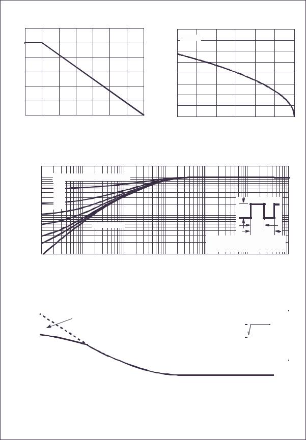
Figure 1. Normalized Power Dissipation vs Ambient Temperature
|
40 |
|
|
|
|
|
|
|
35 |
VGS = 10V |
|
|
|
|
|
|
|
|
|
|
|
|
|
(A) |
30 |
|
|
|
|
|
|
|
|
|
|
|
|
|
|
CURRENT |
25 |
|
|
|
|
|
|
20 |
|
|
|
|
|
|
|
|
|
|
|
|
|
|
|
,DRAIN |
15 |
|
|
|
|
|
|
10 |
|
|
|
|
|
|
|
D |
|
|
|
|
|
|
|
I |
|
|
|
|
|
|
|
|
5 |
|
|
|
|
|
|
|
0 |
|
|
|
|
|
|
|
25 |
50 |
75 |
100 |
125 |
150 |
175 |
|
|
|
TC, CASE TEMPERATURE (oC) |
|
|
||
Figure 2. Maximum Continuous Drain Current vs Case Temperature
|
|
2.0 |
|
|
|
|
|
|
|
|
1.0 |
DUTY CYCLE - DESCENDING ORDER |
|
|
|
|
|
|
|
|
0.5 |
|
|
|
|
|
|
|
|
0.2 |
|
|
|
|
|
|
IMPEDANCE |
|
0.1 |
|
|
|
|
|
NORMALIZED |
|
0.05 |
|
|
|
|
|
|
|
0.02 |
|
|
|
|
|
||
|
0.01 |
|
|
|
PDM |
|
||
|
|
|
|
|
|
|||
0.1 |
|
|
|
|
|
|
||
|
|
|
|
|
|
|
||
, |
THERMAL |
|
|
SINGLE PULSE |
|
|
t1 |
|
θ JC |
|
|
|
|
|
|||
|
|
|
|
|
t2 |
|
||
Z |
|
|
|
|
|
|
||
|
|
|
|
NOTES: |
|
|
||
|
|
|
|
|
|
DUTY FACTOR: D = t1/t2 |
|
|
|
|
|
|
|
|
PEAK TJ = PDM x Zθ JC x Rθ JC + TC |
|
|
|
|
0.01 |
|
|
|
|
|
|
|
|
10-5 |
10-4 |
10-3 |
10-2 |
10-1 |
100 |
101 |
t, RECTANGULAR PULSE DURATION (s)
Figure 3. Normalized Maximum Transient Thermal Impedance
|
500 |
|
|
|
|
|
|
|
|
|
|
|
|
|
|
|
|
|
|
|
|
|
|
|
|
|
|
|
|
|
|
|
|
|
|
|
|
|
|
|
|
|
|
|
|
|
|
|
|
|
|
|
|
|
|
|
|
|
|
|
|
|
|
|
|
|
|
|
|
|
|
|
|
|
|
|
|
|
|
|
|
|
|
|
|
|
|
|
|
|
|
|
|
|
|
|
|
|
|
|
|
|
T |
C = 25oC |
|
|
|
|
|
|
|
|
|
|
|
|
|
||||
|
|
|
|
|
|
|
|
|
|
|
|
|
|
|
|
|
|
|
|
|
|
|
|
|
|
|
|
|
|
|
|
|
|
|
|
|
|
|
|
|
|
|
|
|
|
|
|
|
|
|
|
|
|
|
||||||
|
|
|
|
|
|
|
|
|
|
|
|
|
|
|
|
|
|
|
|
|
|
|
|
|
|
|
|
|
|
|
|
|
|
|
|
|
|
|
|
|
|
FOR TEMPERATURES |
|
|
|
|||||||||||||||
|
|
|
|
|
|
|
|
|
TRANSCONDUCTANCE |
|
|
|
|
|
|
|
|
|
|
|
|
|
|
|
|
|
|
|
|
|
ABOVE 25oC DERATE PEAK |
|
|
|
||||||||||||||||||||||||||
|
|
|
|
|
|
|
|
|
MAY LIMIT CURRENT |
|
|
|
|
|
|
|
|
|
|
|
|
|
|
|
|
|
|
|
|
|
|
|
CURRENT AS FOLLOWS: |
|
|
|
||||||||||||||||||||||||
|
|
|
|
|
|
|
|
|
IN THIS REGION |
|
|
|
|
|
|
|
|
|
|
|
|
|
|
|
|
|
|
|
|
|
|
|
|
|
|
|||||||||||||||||||||||||
(A) |
|
|
|
|
|
|
|
|
|
|
|
|
|
|
|
|
|
|
|
|
|
|
|
|
|
|
|
|
|
|
|
|
|
|
|
|
|
|
|
|
|
|
|
|
|
|
|
|
|
|
||||||||||
|
|
|
|
|
|
|
|
|
|
|
|
|
|
|
|
|
|
|
|
|
|
|
|
|
|
|
|
|
|
|
|
|
|
|
|
|
|
|
|
|
|
I = I25 |
|
175 - TC |
|
|
|
|
||||||||||||
CURRENTPEAK, |
|
|
|
|
|
|
|
|
|
|
|
|
|
|
|
|
|
|
|
|
|
|
|
|
|
|
|
|
|
|
|
|
|
|
|
|
|
|
|
|
|
|
|
|
|
|
|
|
150 |
|
|
|
|
|
|
|
|
|
|
|
DM |
100 |
|
|
|
|
|
|
|
|
|
|
|
|
|
|
|
|
|
|
|
|
|
|
|
|
|
|
|
|
|
|
|
|
|
|
|
|
|
|
|
|
|
|
|
|
|
|
|
|
|
|
|
|
|
|
|
|
|
|
|
|
|
|
|
|
|
|
|
|
|
|
|
|
|
|
|
|
|
|
|
|
|
|
|
|
|
|
|
|
|
|
|
|
|
|
|
|
|
|
|
|
|
|
|
|
|
|
|
|
|
|
|
|
|
|
|
|
|
|
||
|
|
|
|
|
|
|
|
|
|
|
|
|
|
|
|
|
|
|
|
|
|
|
|
|
|
|
|
|
|
|
|
|
|
|
|
|
|
|
|
|
|
|
|
|
|
|
|
|
|
|
|
|
|
|
|
|
|
|
|
|
|
|
|
|
|
|
|
|
|
|
|
|
|
|
|
|
|
|
|
|
|
|
|
|
|
|
|
|
|
|
|
|
|
|
|
|
|
|
|
|
|
|
|
|
|
|
|
|
|
|
|
|
|
|
|
|
|
|
|
|
|
|
|
|
|
|
|
|
|
|
|
|
|
|
|
|
|
|
|
|
|
|
|
|
|
|
|
|
|
|
|
|
|
|
|
|
|
|
|
|
|
|
|
|
|
|
|
|
|
|
|
|
|
|
|
|
|
|
|
|
|
|
|
|
|
|
|
|
|
|
|
|
|
|
|
|
|
|
|
|
|
|
|
|
|
|
|
|
|
|
|
|
|
|
|
|
|
|
|
|
|
|
|
|
|
|
|
|
|
|
|
|
|
|
|
|
|
|
|
|
|
|
|
|
|
|
|
|
|
|
|
|
|
|
|
|
|
|
|
|
|
|
|
|
|
|
|
|
|
|
|
|
|
|
|
|
|
|
|
|
|
|
|
|
|
|
|
|
|
|
|
|
|
|
|
|
|
|
|
|
|
|
|
|
|
|
|
|
|
|
|
|
|
|
|
|
|
|
|
|
|
|
|
|
|
|
|
|
|
|
|
|
|
|
|
|
|
|
|
|
|
|
|
|
|
|
|
|
|
|
|
|
|
|
|
|
|
|
|
|
|
|
|
|
|
I |
|
|
|
|
|
|
|
|
|
|
|
|
|
|
|
|
|
|
|
|
|
|
|
|
|
|
|
|
|
|
|
|
|
|
|
|
|
|
|
|
|
|
|
|
|
|
|
|
|
|
|
|
|
|
|
|
|
|
|
|
|
|
|
|
|
|
|
|
|
|
|
|
|
|
|
|
|
|
|
|
|
|
|
|
|
|
|
|
|
|
|
|
|
|
|
|
|
|
|
|
|
|
|
|
|
|
|
|
|
|
|
|
|
|
|
|
|
|
|
|
|
|
20 |
|
VGS = 10V |
|
|
|
|
|
|
|
|
|
|
|
|
|
|
|
|
|
|
|
|
|
|
|
|
|
|
|
|
|
|
|
|
|
|
|
|
|
|
|
|
|
|
|
|
|
|
|
|
|
|
|
|
|
|
|
||
|
|
|
|
|
|
|
|
|
|
|
|
|
|
|
|
|
|
|
|
|
|
|
|
|
|
|
|
|
|
|
|
|
|
|
|
|
|
|
|
|
|
|
|
|
|
|
|
|
|
|
|
|
|
|
|
|
|
|
|
|
|
|
|
|
|
|
|
|
|
|
|
|
|
|
|
|
|
|
|
|
|
|
|
|
|
|
|
|
|
|
|
|
|
|
|
|
|
|
|
|
|
|
|
|
|
|
|
|
|
|
|
|
|
|
|
|
|
|
|
|
|
|
10-5 |
|
|
|
|
|
10-4 |
|
|
|
|
|
10-3 |
10-2 |
|
10-1 |
|
100 |
101 |
|||||||||||||||||||||||||||||||||||||||||
|
|
|
|
|
|
|
|
|
|
|
|
|
|
|
|
|
|
|
|
|
|
|
t, PULSE WIDTH (s) |
|
|
|
|
|
|
|
|
|
|
|
|
|
|
|
|
|
|
|
|
|
|
|
|
|
|
|
|
|||||||||
Figure 4. Peak Current Capability
FDU2572 / FDD2572
©2002 Fairchild Semiconductor Corporation |
FDD2572 / FDU2572 Rev. B |

Typical Characteristics TC = 25°C unless otherwise noted |
|
|
|
|
|
|
|
|
|
|
FDD2572 |
||||||||||||||
|
1000 |
|
|
|
|
|
|
|
|
|
|
|
100 |
|
|
|
|
|
|
|
|
|
|
||
|
|
|
|
|
|
|
|
|
10 s |
|
|
|
|
|
|
|
|
|
STARTING T |
|
= 25oC |
|
|||
|
|
|
|
|
|
|
|
|
|
|
AVALANCHE CURRENT (A) |
|
|
|
|
|
|
J |
|
FDU2572 / |
|||||
|
|
|
|
|
|
|
|
|
|
|
|
|
|
|
|
|
|
|
|
|
|
|
|||
(A) |
100 |
|
|
|
|
|
|
|
100 s |
|
|
|
|
|
|
|
|
|
|
|
|
|
|
||
CURRENT |
|
|
|
|
|
|
|
|
|
|
|
10 |
|
|
|
|
|
|
|
|
|
|
|||
10 |
|
|
|
|
|
|
|
1ms |
|
|
|
|
|
|
|
|
|
|
|
|
|
|
|||
|
|
|
|
|
|
|
|
|
|
|
|
|
|
|
|
|
|
|
|
|
|
||||
|
|
|
|
|
|
|
|
|
|
|
|
|
|
|
|
|
|
|
|
|
|
|
|||
, DRAIN |
|
OPERATION IN THIS |
|
|
|
|
|
|
|
|
|
STARTING TJ = 150oC |
|
|
|
|
|
||||||||
|
AREA MAY BE |
|
|
|
10ms |
|
|
1 |
|
|
|
|
|
|
|
||||||||||
|
LIMITED BY rDS(ON) |
|
|
|
|
|
|
|
|
|
|
|
|
|
|
|
|
|
|||||||
D |
1 |
|
|
|
|
|
|
|
|
|
|
|
|
|
|
|
|
|
|
|
|
|
|
||
I |
|
|
|
|
|
|
|
|
|
|
|
|
If R = 0 |
|
|
|
|
|
|
|
|||||
|
|
|
|
|
|
|
|
|
|
|
|
, |
|
|
|
|
|
|
|
|
|
|
|||
|
|
SINGLE PULSE |
|
|
|
|
|
|
|
|
|
tAV = (L)(IAS)/(1.3*RATED BVDSS - VDD) |
|
|
|
|
|||||||||
|
|
|
|
|
|
DC |
|
|
AS |
|
|
|
|
|
|
||||||||||
|
|
TJ = MAX RATED |
|
|
|
|
|
|
I |
|
|
If R ≠ |
0 |
|
|
|
|
|
|
|
|
||||
|
|
|
|
|
|
|
|
|
|
|
|
|
|
|
|
|
|
|
|
||||||
|
|
T = 25oC |
|
|
|
|
|
|
|
|
|
|
|
tAV = (L/R)ln[(IAS*R)/(1.3*RATED BVDSS - VDD) +1] |
|
||||||||||
|
|
C |
|
|
|
|
|
|
|
|
|
|
0.1 |
|
|
|
|
|
|
|
|
|
|
|
|
|
0.1 |
|
|
|
|
|
|
|
|
|
|
|
|
|
|
|
|
|
|
|
|
|
|
||
|
1 |
|
|
|
10 |
|
|
|
|
100 |
200 |
|
|
0.001 |
|
|
|
0.01 |
|
0.1 |
|
1 |
|||
|
|
|
|
VDS, DRAIN TO SOURCE VOLTAGE (V) |
|
|
|
|
|
|
|
|
tAV, TIME IN AVALANCHE (ms) |
|
|
||||||||||
|
Figure 5. Forward Bias Safe Operating Area |
NOTE: Refer to Fairchild Application Notes AN7514 and AN7515 |
|||||||||||||||||||||||
|
|
|
|
|
|
|
|
|
|
|
|
|
Figure 6. Unclamped Inductive Switching |
|
|||||||||||
|
|
|
|
|
|
|
|
|
|
|
|
|
|
|
|
|
|
|
Capability |
|
|
|
|
||
|
60 |
PULSE DURATION = 80 s |
|
|
|
|
|
|
|
60 |
|
|
|
|
|
|
|
|
|
|
|
|
|||
|
|
|
|
|
|
|
|
|
|
T |
|
= 25oC |
|
V |
= 10V |
|
|
|
|
||||||
|
|
DUTY CYCLE = 0.5% MAX |
|
|
|
|
|
|
|
|
C |
|
|
|
|
|
|||||||||
|
50 |
|
|
|
|
|
|
|
50 |
|
|
|
|
GS |
|
|
|
|
|
|
|||||
|
VDD = 15V |
|
|
|
|
|
|
|
|
|
|
|
|
|
|
|
|
|
|
|
|
|
|
||
(A) |
40 |
|
|
|
|
|
|
|
|
|
|
(A) |
40 |
|
|
|
|
|
|
|
|
|
|
|
|
CURRENT |
|
|
|
|
|
|
|
|
|
|
CURRENT |
|
|
|
|
|
|
|
|
|
VGS = 7V |
|
|||
|
|
|
|
T |
= 175oC |
|
|
|
|
|
|
|
|
|
|
|
|
|
|
|
|
||||
|
|
|
|
|
|
|
|
|
|
|
|
|
|
|
|
|
|
|
|
|
|
||||
|
|
|
|
J |
|
|
|
|
|
|
|
|
|
|
|
|
|
|
VGS = 6V |
|
|
|
|
||
30 |
|
|
|
|
|
|
|
|
|
|
30 |
|
|
|
|
|
|
|
|
|
|
|
|||
|
|
|
|
|
|
|
|
|
|
|
|
|
|
|
|
|
|
|
|
|
|
||||
|
|
|
|
|
|
|
|
|
|
|
|
|
|
|
|
|
|
|
|
|
|
|
|
||
, DRAIN |
20 |
T |
J |
= 25oC |
|
|
|
|
|
|
|
,DRAIN |
20 |
|
|
|
|
|
V |
|
= 5V |
|
|
|
|
|
|
|
|
|
|
|
|
|
|
|
|
|
|
|
|
GS |
|
|
|
|
|
||||
|
|
|
|
|
|
|
|
o |
|
|
|
|
|
|
|
|
|
|
|
|
|
|
|
||
D |
|
|
|
|
|
|
T |
J |
= -55 C |
|
D |
|
|
|
|
|
|
|
|
|
|
|
|
|
|
I |
10 |
|
|
|
|
|
|
|
|
|
I |
10 |
|
|
|
|
|
|
|
|
|
|
|
|
|
|
|
|
|
|
|
|
|
|
|
|
|
|
|
|
|
|
|
|
PULSE DURATION = 80 s |
|
|||||
|
|
|
|
|
|
|
|
|
|
|
|
|
|
|
|
|
|
|
|
|
|
||||
|
|
|
|
|
|
|
|
|
|
|
|
|
|
|
|
|
|
|
|
|
DUTY CYCLE = 0.5% MAX |
|
|||
|
0 |
|
|
|
|
|
|
|
|
|
|
|
0 |
|
|
|
|
|
|
|
|
|
|
|
|
|
3.0 |
3.5 |
|
4.0 |
4.5 |
5.0 |
5.5 |
6.0 |
6.5 |
|
|
0 |
|
|
1 |
|
2 |
|
3 |
|
4 |
|
5 |
||
|
|
|
|
VGS , GATE TO SOURCE VOLTAGE (V) |
|
|
|
|
|
|
|
VDS , DRAIN TO SOURCE VOLTAGE (V) |
|
|
|||||||||||
|
|
Figure 7. Transfer Characteristics |
|
|
|
Figure 8. |
Saturation Characteristics |
|
|||||||||||||||||
|
60 |
PULSE DURATION = 80 s |
|
|
|
|
|
|
|
|
3.0 |
|
|
|
|
|
|
|
|
|
|
|
|||
|
|
|
|
|
|
|
|
|
|
|
PULSE DURATION = 80 s |
|
|
|
|
|
|
||||||||
|
|
DUTY CYCLE = 0.5% MAX |
|
|
|
|
|
|
|
|
|
|
|
|
|
|
|
||||||||
) |
|
|
|
|
|
|
|
|
|
|
DUTY CYCLE = 0.5% MAX |
|
|
|
|
|
|
||||||||
TO SOURCE ON RESISTANCE (m Ω |
|
|
|
|
|
|
|
|
|
|
|
NORMALIZED DRAIN TO SOURCE |
|
2.5 |
|
|
|
|
|
|
|||||
|
|
|
|
|
|
|
|
|
|
|
|
|
|
|
|
|
|
|
|
|
|
|
|||
55 |
|
|
|
VGS = 6V |
|
|
|
|
|
|
|
|
|
|
|
|
|
|
|
|
|
|
|||
|
|
|
|
|
|
|
|
|
|
|
ON RESISTANCE |
2.0 |
|
|
|
|
|
|
|
|
|
|
|
||
50 |
|
|
|
|
|
|
|
|
|
|
1.5 |
|
|
|
|
|
|
|
|
|
|
|
|||
|
|
|
|
|
|
|
|
|
|
|
|
|
|
|
|
|
|
|
|
|
|
||||
|
|
|
|
VGS = 10V |
|
|
|
|
|
|
|
|
|
|
|
|
|
|
|
|
|
||||
|
|
|
|
|
|
|
|
|
|
|
1.0 |
|
|
|
|
|
|
|
|
|
|
|
|||
45 |
|
|
|
|
|
|
|
|
|
|
|
|
|
|
|
|
|
|
|
|
|
|
|||
|
|
|
|
|
|
|
|
|
|
|
0.5 |
|
|
|
|
|
|
|
|
|
|
|
|||
|
|
|
|
|
|
|
|
|
|
|
|
|
|
|
|
|
|
VGS = 10V, ID =9A |
|
||||||
DRAIN |
40 |
|
|
|
|
|
|
|
|
|
|
|
|
0 |
|
|
|
|
|
|
|
|
|
|
|
|
|
|
|
|
|
|
|
|
|
|
|
|
|
|
|
|
|
|
|
|
|
|
|
||
0 |
|
|
|
10 |
|
20 |
|
|
|
30 |
|
|
-80 |
|
-40 |
0 |
40 |
|
80 |
|
120 |
160 |
200 |
||
|
|
|
|
|
|
|
|
|
|
|
|
|
|||||||||||||
|
|
|
|
|
ID, DRAIN CURRENT (A) |
|
|
|
|
|
|
|
|
|
TJ, JUNCTION TEMPERATURE (oC) |
|
|
||||||||
Figure 9. Drain to Source On Resistance vs Drain |
|
Figure 10. Normalized Drain to Source On |
|
||||||||||||||||||||||
|
|
|
|
|
Current |
|
|
|
|
|
|
|
Resistance vs Junction Temperature |
|
|||||||||||
©2002 Fairchild Semiconductor Corporation |
|
|
|
|
|
|
|
|
|
|
|
|
|
|
|
|
|
FDD2572 / FDU2572 Rev. B |
|||||||
 Loading...