


November 1988
Revised December 1998
74AC646 • 74ACT646
Octal Transceiver/Register with 3-STATE Outputs
General Description
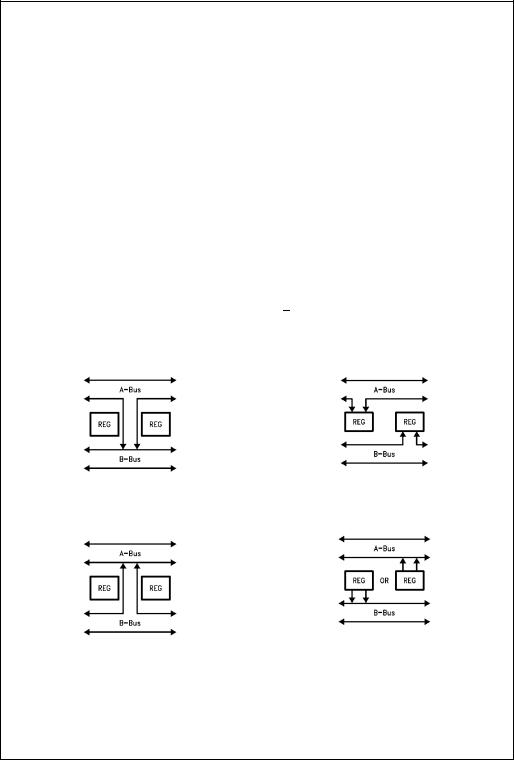
The AC/ACT646 consist of registered bus transceiver circuits, with outputs, D-type flip-flops and control circuitry providing multiplexed transmission of data directly from the input bus or from the internal storage registers. Data on the A or B bus will be loaded into the respective registers on the LOW-to-HIGH transition of the appropriate clock pin (CPAB or CPBA). The four fundamental data handling functions available are illustrated in Figure 1, Figure 2, Figure 3, and Figure 4.
Features
■Independent registers for A and B buses
■Multiplexed real-time and stored data transfers
■3-STATE outputs
■300 mil dual-in-line package
■Outputs source/sink 24 mA
■ACT646 has TTL compatible inputs
Ordering Code:
Order Number |
Package Number |
Package Description |
|
|
|
74AC646SC |
M24B |
24-Lead Small Outline Integrated Circuit (SOIC), JEDEC MS-013, 0.300” Wide Body |
|
|
|
74AC646SPC |
N24C |
24-Lead Plastic Dual-In-Line Package (PDIP), JEDEC MS-100, 0.300” Wide |
|
|
|
74ACT646SPC |
N24C |
24-Lead Plastic Dual-In-Line Package (PDIP), JEDEC MS-100, 0.300” Wide |
|
|
|
Device also available in Tape and Reel. Specify by appending suffix letter “X” to the ordering code.
Logic Symbols |
Connection Diagram |
Pin Assignment for DIP and SOIC
IEEE/IEC
Pin Descriptions
|
Pin Names |
Description |
|
|
|
|
|
|
A0–A7 |
Data Register A Inputs |
|
|
|
|
Data Register A Outputs |
|
B0–B7 |
Data Register B Inputs |
|
|
|
|
Data Register B Outputs |
|
CPAB, CPBA |
Clock Pulse Inputs |
|
|
SAB, SBA |
Transmit/Receive Inputs |
|
|
|
|
Output Enable Input |
|
G |
||
|
DIR |
Direction Control Input |
|
|
|
|
|
FACTä is a trademark of Fairchild Semiconductor Corporation.
Outputs STATE-3 with Transceiver/Register Octal 74ACT646 • 74AC646
© 1999 Fairchild Semiconductor Corporation |
DS010132.prf |
www.fairchildsemi.com |
74AC646 • 74ACT646
Function Table
|
|
|
Inputs |
|
|
Data I/O (Note 1) |
Function |
||
|
|
|
|
|
|
|
|
|
|
|
|
DIR |
CPAB CPBA |
SAB |
SBA |
A0–A 7 |
B0–B 7 |
|
|
G |
|
||||||||
|
|
|
|
|
|
|
|
|
|
|
H |
X |
H or L |
H or |
X |
X |
|
|
Isolation |
|
|
|
|
L |
|
|
|
|
|
|
H |
X |
|
X |
X |
X |
Input |
Input |
Clock An Data into A Register |
|
H |
X |
X |
|
X |
X |
|
|
Clock Bn Data into B Register |
|
|
|
|
|
|
|
|
|
|
|
L |
H |
X |
X |
L |
X |
|
|
An to Bn—Real Time (Transparent Mode) |
|
L |
H |
|
X |
L |
X |
Input |
Output |
Clock An Data into A Register |
|
L |
H |
H or L |
X |
H |
X |
|
|
A Register to Bn (Stored Mode) |
|
L |
H |
|
X |
H |
X |
|
|
Clock An Data into A Register and Output to Bn |
|
L |
L |
X |
X |
X |
L |
|
|
Bn to An —Real Time (Transparent Mode) |
|
L |
L |
X |
|
X |
L |
Output |
Input |
Clock Bn Data into B Register |
|
L |
L |
X |
H or L |
X |
H |
|
|
B Register to An (Stored Mode) |
|
L |
L |
X |
|
X |
H |
|
|
Clock Bn Data into B Register and Output to An |
|
|
|
|
|
|
|
|
|
|
H = HIGH Voltage Level
L = LOW Voltage Level
X = Immaterial
= LOW-to-HIGH Transition
Note 1: The data output functions may be enabled or disabled by various signals at the G and DIR inputs. Data input functions are always enabled; i.e., data at the bus pins will be stored on every LOW-to-HIGH transition of the appropriate clock inputs.
Real Time Transfer |
Storage from |
A-Bus to B-Bus |
Bus to Register |
FIGURE 3.
FIGURE 1.
Real Time Transfer
Transfer from
B-Bus to A-Bus
Register to Bus
FIGURE 4.
FIGURE 2.
www.fairchildsemi.com |
2 |

Logic Diagram
Please note that this diagram is provided only for the understanding of logic operations and should not be used to estimate propagation delays.
74ACT646 • 74AC646
3 |
www.fairchildsemi.com |
 Loading...