


74AC520SCX
© 1999 Fairchild Semiconductor Corporation DS010194 www.fairchildsemi.com
February 1989
Revised November 1999
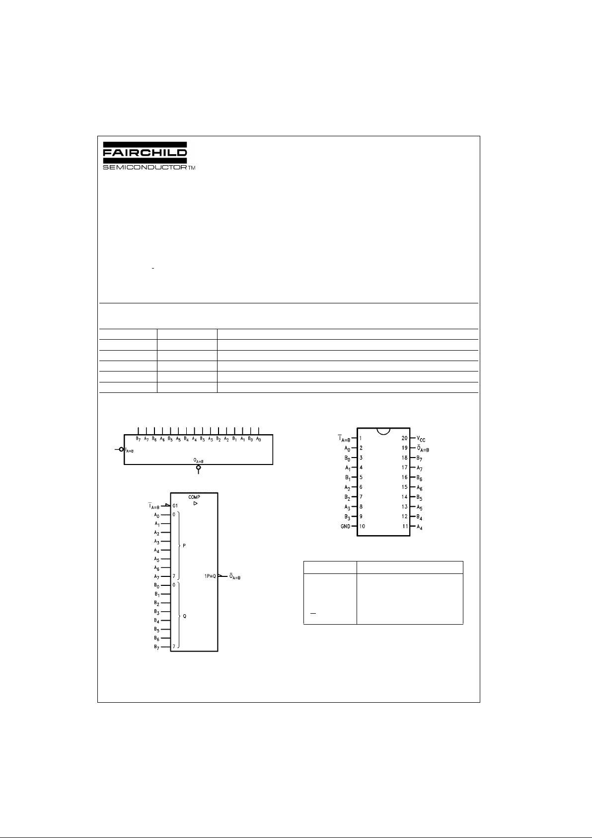
74AC520 • 74ACT520 8-Bit Identity Comparator
74AC520 • 74ACT520
8-Bit Identity Comparator
General Description
The AC/ACT520 are exp andable 8-bit compara tors. They
compare two words of up to e ight bits each an d provide a
LOW output when the two words match bit for bit. The
expansion input I
A = B
also serves as an active LOW enable
input.
Features
■ Compares two 8-bit words in 6.5 ns typ
■ Expandable to any word length
■ 20-pin package
■ Outputs source/sink 24 mA
■ ACT520 has TTL-compatible inputs
Ordering Code:
Device also available in Tape and Reel. Specify by appending s uffix let te r “X” to the ordering code.
Logic Symbols
IEEE/IEC
Connection Diagram
Pin Descriptions
FACT is a trademark of Fairchild Semiconductor Corporation.
Order Number Package Number Package Description
74AC520SC M20B 20-Lead Small Outline Integrated Circuit (SOIC), JEDEC MS-013, 0.300” Wide Body
74AC520PC N20A 20-Lead Plastic Dual-In-Line Package (PDIP), JEDEC MS-001, 0.300” Wide
74ACT520SC M20B 20-Lead Small Outline Integrated Circuit (SOIC), JEDEC MS-013, 0.300” Wide Body
74ACT520SJ M20D 20-Lead Small Outline Package (SOP), EIAJ TYPE II, 5.3mm Wide
74ACT520PC N20A 20-Lead Plastic Dual-In-Line Package (PDIP), JEDEC MS-001, 0.300” Wide
Pin Names Description
A
0
–A
7
Word A Inputs
B
0
–B
7
Word B Inputs
T
A = B
Expansion or Enable Input
O
A = B
Identity Output
www.fairchildsemi.com 2
74AC520 • 74ACT520
Truth Table
H = HIGH Voltage Level
L = LOW Voltage Level
Note 1: *A
0
= B
0
, A
1
= B
1
, A
2
= B
2
, etc.
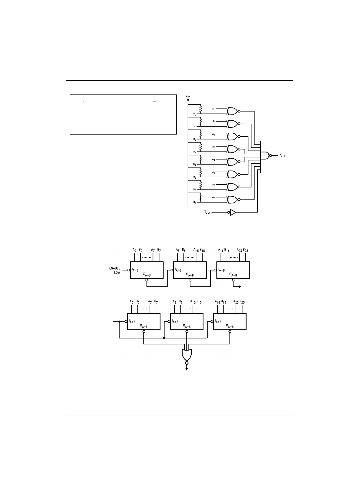
Logic Diagram
Please note that this diagram is provided only for the understanding of logic
operations and should not be used to estimate propagation delays.
Applications
Ripple Expansion
Parallel Expansion
Inputs Outputs
I
A = B
A, B O
A = B
LA = B (Note 1) L
LA ≠ Β H
HA = B (Note 1) H
HA ≠ Β H
3 www.fairchildsemi.com
74AC520 • 74ACT520
Absolute Maximum Ratings(Note 2) Recommended Operating
Conditions
Note 2: Absolute max imum ratings are those values beyond w hich damage
to the device may occu r. The databook spe cificatio ns shou ld be met, wit h-
out exception, to ensure that the system de sign is relia ble over its p ower
supply, temperature, and output/input loading variables. Fairchild does not
recommend operation of FACT circuits outside databook specif ic at ions.
DC Electrical Characteristics for AC
Note 3: All outputs loaded; thres holds on input associate d w it h output under test.
Note 4: Maximum test duration 2.0 ms, one output loaded at a time.
Note 5: I
IN
and I
CC
@ 3.0V are guaranteed to be less than or equa l t o th e respective limit @ 5.5V V
CC
.
Supply Voltage (V
CC
) −0.5V to +7.0V
DC Input Diode Current (I
IK
)
V
I
= −0.5V −20 mA
V
I
= V
CC
+ 0.5V +20 mA
DC Input Voltage (V
I
) −0.5V to V
CC
+ 0.5V
DC Output Diode Current (I
OK
)
V
O
= −0.5V −20 mA
V
O
= V
CC
+ 0.5V +20 mA
DC Output Voltage (V
O
) −0.5V to V
CC
+ 0.5V
DC Output S ource
or Sink Current (I
O
) ±50 mA
DC V
CC
or Ground Current
per Output Pin (I
CC
or I
GND
) ±50 mA
Storage Temperature (T
STG
) −65°C to +150°C
Junction Temperature (T
J
)
PDIP 140°C
Supply Voltage (V
CC
)
AC 2.0V to 6.0V
ACT 4.5V to 5.5V
Input Voltage (V
I
)0V to V
CC
Output Voltage (V
O
)0V to V
CC
Operating Temperature (T
A
) −40°C to +85°C
Minimum Input Edge Rate (∆V/∆t)
AC Devices
V
IN
from 30% to 70% of V
CC
V
CC
@ 3.3V, 4.5V, 5.5V 125 mV/ns
Minimum Input Edge Rate (∆V/∆t)
ACT Devices
V
IN
from 0.8V to 2.0V
V
CC
@ 4.5V, 5.5V 125 mV/ns
Symbol Parameter
V
CC
T
A
= +25°C T
A
= −40°C to +85°C
Units Conditions
(V) Typ Guaranteed Limits
V
IH
Minimum HIGH Level 3.0 1.5 2.1 2.1 V
OUT
= 0.1V
Input Voltage 4.5 2.25 3.15 3.15 V or V
CC
− 0.1V
5.5 2.75 3.85 3.85
V
IL
Maximum LOW Level 3.0 1.5 0.9 0.9 V
OUT
= 0.1V
Input Voltage 4.5 2.25 1.35 1.35 V or V
CC
− 0.1V
5.5 2.75 1.65 1.65
V
OH
Minimum HIGH Level 3.0 2.99 2.9 2.9
Output Voltage 4.5 4.49 4.4 4.4 V I
OUT
= −50 µA
5.55.495.4 5.4
V
IN
= V
IL
or V
IH
3.0 2.56 2.46 I
OH
= −12 mA
4.5 3.86 3.76 V I
OH
= −24 mA
5.5 4.86 4.76 I
OH
= −24 mA (Note 3)
V
OL
Maximum LOW Level 3.0 0.002 0.1 0.1
Output Voltage 4.5 0.001 0.1 0.1 V I
OUT
= 50 µA
5.5 0.001 0.1 0.1
V
IN
= V
IL
or V
IH
3.0 0.36 0.44 I
OL
= 12 mA
4.5 0.36 0.44 V I
OL
= 24 mA
5.5 0.36 0.44 I
OL
= 24 mA (Note 3)
I
IN
(Note 5) Maximum Input Leakage Current 5.5 ±0.1 ±1.0 µAV
I
= V
CC
, GND, A Inputs Only
I
IH
Maximum Input HIGH Leakage Current 5.5 10.0 10.0 µAV
I
= V
CC
, B Inputs Only
I
IL
Maximum Input LOW Leakage Current 5.5 −0.3 −0.6 −1.0 mA V
I
= V
CC
, B Inputs Only
I
OLD
Minimum Dynamic 5.5 75 mA V
OLD
= 1.65V Max
I
OHD
Output Current (Note4) 5.5 −75 mA V
OHD
= 3.85V Min
I
CC
Maximum Quiescent Supply Current 5.5 4.0 40.0 µAV
IN
= V
CC
I
CC
(Note 5) Maximum Quiescent Supply Current 5.5 2.3 4.8 8.0 mA V
IN
= GND
 Loading...