


74AC574SJX
Fairchild Semiconductor 74AC574SJX, 74AC574SJ, 74AC574SCX, 74AC574SC, 74AC574PC Datasheet
...
© 1999 Fairchild Semiconductor Corporation DS009910 www.fairchildsemi.com
September 1988
Revised November 1999
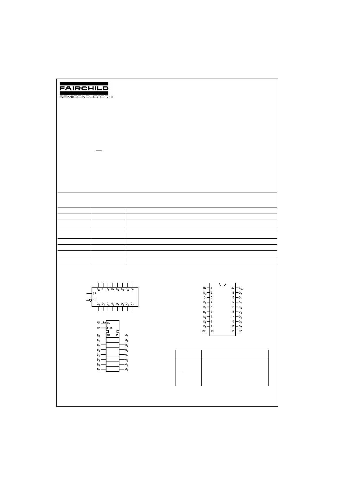
74AC574 • 74ACT574 Octal D-Type Flip-Flop with 3-STATE Outputs
74AC574 • 74ACT574
Octal D-Type Flip-Flop with 3-STATE Outputs
General Description
The AC/ACT574 is a high-speed, low power octal flip-flop
with a buffered common C lock (CP) and a buffered com mon Output Enable (OE
). The information presented to the
D-type inputs is stored in the flip-flops on the LOW-to-HIGH
Clock (CP) transition.
The AC/ACT574 is functionally identical to the AC /ACT3 74
except for the pinouts.
Features
■ ICC and IOZ reduced by 5 0%
■ Inputs and outputs on opposite sides of package
allowing easy interface with microprocessors
■ Useful as input or output port for microprocessors
■ Functionally identical to AC/ACT374
■ 3-STATE outputs for bus-oriented applications
■ Outputs source/sink 24 mA
■ ACT574 has TTL-compatible inputs
Ordering Code:
Device also available in Tape and Reel. Specify by appending s uffix let te r “X” to the ordering code.
Logic Symbols
IEEE/IEC
Connection Diagram
Pin Descriptions
FACT is a trademark of Fairchild Semiconductor Corporation.
Order Number Package Number Package Description
74AC574SC M20B 20-Lead Small Outline Integrated Circuit (SOIC), JEDEC MS-013, 0.300” Wide Body
74AC574SJ M20D 20-Lead Small Outline Package (SOP), EIAJ TYPE II, 5.3mm Wide
74AC574MTC MTC20 20-Lead Thin Shrink Small Outline Package (TSSOP), JEDEC MO-153, 4.4mm Wide
74AC574PC N20A 20-Lead Plastic Dual-In-Line Package (PDIP), JEDEC MS-001, 0.300” Wide
74ACT574SC M20B 20-Lead Small Outline Integrated Circuit (SOIC), JEDEC MS-01
74ACT574SJ M20D 20-Lead Small Outline Package (SOP), EIAJ TYPE II, 5.3mm Wide
74ACT574MTC MTC20 20-Lead Thin Shrink Small Outline Package (TSSOP), JEDEC MO-153, 4.4mm Wide
74ACT574PC N20A 20-Lead Plastic Dual-In-Line Package (PDIP), JEDEC MS-001, 0.300” Wide
Pin Names Description
D
0–D7
Data Inputs
CP Clock Pulse Input
OE
3-STATE Output Enable Input
O
0–O7
3-STATE Outputs
www.fairchildsemi.com 2
74AC574 • 74ACT574
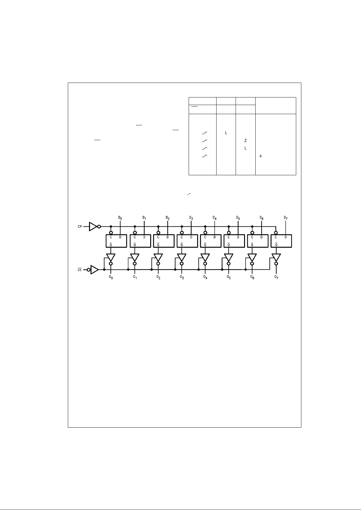
Functional Description
The AC/ACT574 consists o f eight edge-trig gered flip-flops
with individual D-type inputs and 3-STATE true outputs.
The buffered clock and buffered Output Enable are common to all flip-flops. The eight flip-flops will store the state
of their individu al D-type inputs that meet the se tup and
hold time requiremen ts on the LOW-to-HIGH Clock (CP)
transition. With the Output Enab le (OE
) LOW, the contents
of the eight flip-flops are available at the outputs. When OE
is HIGH, the outputs go to the high impedance state. Operation of the OE
input does not affect the state of the flip-
flops.
Function Table
H = HIGH Voltage Level
L = LOW Voltage Level
X = Immaterial
Z = High Impedance
= LOW-to-HIGH Transition
NC = No Change
Logic Diagram
Please note that this diagram is provided only for the understanding of logic operations and should not be used to estimate propagation delays.
Inputs Internal Outputs
Function
OE CP D Q O
N
HHL NC Z Hold
H HH NC Z Hold
H
L L Z Load
H
H H Z Load
L
L L L Data Available
L
H H H Data Available
L H L NC NC No Change in Data
L H H NC NC No Change in Data
3 www.fairchildsemi.com
74AC574 • 74ACT574
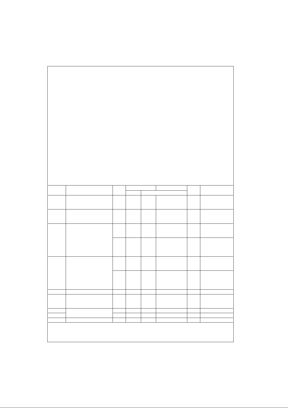
Absolute Maximum Ratings(Note 1) Recommended Operating
Conditions
Note 1: Absolute max imum ratings are those values beyond which damage
to the device may occu r. The databook spe cificatio ns shou ld be met, wit hout exception, to ensure that the system de sign is relia ble over its p ower
supply, temperature, and output/input loading variables. Fairchild does not
recommend operation of FACT circuits outside databook specif ications.
DC Electrical Characteristics for AC
Note 2: All outputs loaded; thres holds on input associate d w it h output under test.
Note 3: Maximum test duration 2.0 ms, one output loaded at a time.
Note 4: I
IN
and ICC @ 3.0V are guaranteed to be less than or equa l t o th e respective limit @ 5.5V VCC.
Supply Voltage (VCC) −0.5V to +7.0V
DC Input Diode Current (I
IK
)
V
I
= −0.5V −20 mA
V
I
= VCC +0.5V +20 mA
DC Input Voltage (V
I
) −0.5V to VCC +0.5V
DC Output Diode Current (I
OK
)
V
O
= −0.5V −20 mA
V
O
= VCC +0.5V +20 mA
DC Output Voltage (V
O
) −0.5V to VCC +0.5V
DC Output Source
or Sink Current (I
O
) ±50 mA
DC V
CC
or Ground Current
Per Output Pin (I
CC
or I
GND
) ±50 mA
Storage Temperature (T
STG
) −65°C to +150°C
Junction Temperature (T
J
)
PDIP 140°C
Supply Voltage (V
CC
)
AC 2.0V to 6.0V
ACT 4.5V to 5.5V
Input Voltage (V
I
)0V to V
CC
Output Voltage (VO)0V to V
CC
Operating Temperature (TA) −40°C to +85°C
Minimum Input Edge Rate (∆V/∆t)
AC Devices
V
IN
from 30% to 70% of V
CC
VCC @ 3.3V, 4.5V, 5.5V 125 mV/ns
Minimum Input Edge Rate (∆V/∆t)
ACT Devices
V
IN
from 0.8V to 2.0V
V
CC
@ 4.5V, 5.5V 125 mV/ns
Symbol Parameter
V
CC
TA = 25°CTA = −40°C to +85°C
Units Conditions
(V) Typ Guaranteed Limits
V
IH
Minimum HIGH Level 3.0 1.5 2.1 2.1 V
OUT
= 0.1V
Input Voltage 4.5 2.25 3.15 3.15 V or VCC − 0.1V
5.5 2.75 3.85 3.85
V
IL
Maximum LOW Level 3.0 1.5 0.9 0.9 V
OUT
= 0.1V
Input Voltage 4.5 2.25 1.35 1.35 V or VCC − 0.1V
5.5 2.75 1.65 1.65
V
OH
Minimum HIGH Level 3.0 2.99 2.9 2.9
Output Voltage 4.5 4.49 4.4 4.4 V I
OUT
= −50 µA
5.5 5.49 5.4 5.4
3.0 2.56 2.46 VIN = VIL or V
IH
4.5 3.86 3.76 V IOH = −12 mA
5.5 4.86 4.76 I
OH
= −24 mA I
OH
IOH = −24 mA (Note 2)
V
OL
Maximum LOW Level 3.0 0.002 0.1 0.1
Output Voltage 4.5 0.001 0.1 0.1 V I
OUT
= 50 µA
5.5 0.001 0.1 0.1
VIN = VILor V
IH
3.0 0.36 0.44 IOL = 12 mA
4.5 0.36 0.44 V IOL = 24 mA
5.5 0.36 0.44 IOL = 24 mA (Note 2)
IIN (Note 4) Maximum Input Leakage Current 5.5 ±0.1 ±1.0 µAVI = VCC, GND
I
OZ
Maximum VI (OE) = VIL, V
IH
3-STATE 5.5 ±0.25 ±2.5 µAVI = VCC, V
GND
Leakage Current VO = VCC, GND
I
OLD
Minimum Dynamic 5.5 75 mA V
OLD
= 1.65V
I
OHD
Output Current (Note 3) 5.5 −75 mA V
OHD
= 3.85V
ICC (Note 4) MaximumQuiescent Supply Current 5.5 4.0 40.0 µAVIN = VCC or GND
 Loading...