


OP221EZ
Table of contents
 Loading...
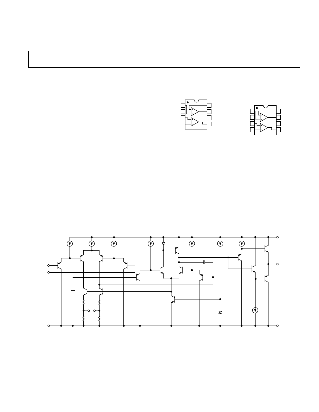
REV. A
Information furnished by Analog Devices is believed to be accurate and
reliable. However, no responsibility is assumed by Analog Devices for its
use, nor for any infringements of patents or other rights of third parties that
may result from its use. No license is granted by implication or otherwise
under any patent or patent rights of Analog Devices.
a
OP221
One Technology Way, P.O. Box 9106, Norwood, MA 02062-9106, U.S.A.
Tel: 781/329-4700 www.analog.com
Fax: 781/326-8703 © Analog Devices, Inc., 2002
Dual Low Power Operational Amplifier,
Single or Dual Supply
FEATURES
Excellent TCVos Match, 2 V/ⴗC Max
Low Input Offset Voltage, 150 V Max
Low Supply Current, 550 A Max
Single Supply Operation, 5 V to 30 V
Low Input Offset Voltage Drift, 0.75 V/ⴗC
High Open-Loop Gain, 1500 V/mV Min
High PSRR, 3 V/V
Wide Common-Mode Voltage
Range, V– to within 1.5 V of V+
Pin Compatible with 1458, LM158, LM2904
Available in Die Form
GENERAL DESCRIPTION
The OP221 is a monolithic dual operational amplifier that can
be used either in single or dual supply operation. The wide
supply voltage range, wide input voltage range, and low supply
current drain of the OP221 make it well-suited for operation
from batteries or unregulated power supplies.
The excellent specifications of the individual amplifiers combined
with the tight matching and temperature tracking between channels
SIMPLIFIED SCHEMATIC
Q1
–IN
+IN
*
ACCESSIBLE IN CHIP FORM ONLY
Q3 Q4
Q5
Q6
Q2
Q7
Q9 Q10
Q12
Q11
Q4
Q13
NULL
*
Q26
Q28
Q27
Q29
Q33
V+
OUTPUT
V–
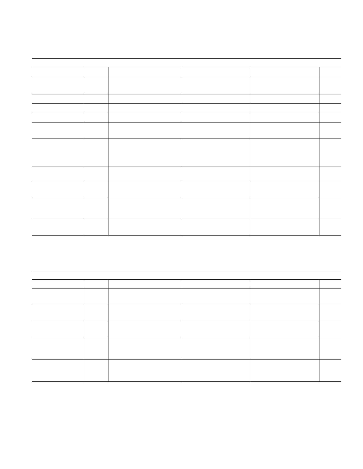
8-Lead SO
(S-Suffix)
8
7
6
5
1
2
3
4
NC = NO CONNECT
+IN A
V–
+IN B
–IN A
OUT A
V+
OUT B–IN B
8-Lead
HERMETIC DIP
(Z-Suffix)
8
7
6
5
1
2
3
4
NC = NO CONNECT
+IN A
V–
+IN B
–IN A
OUT A
V+
–IN B
OUT B
PIN CONNECTIONS
provide high performance in instrumentation amplifier designs.
The individual amplifiers feature very low input offset voltage,
low offset voltage drift, low noise voltage, and low bias current.
They are fully compensated and protected.
Matching between channels is provided on all critical parameters
including input offset voltage, tracking of offset voltage vs. tem-
perature, non-inverting bias currents, and common-mode rejection.

REV. A
–2–
OP221–SPECIFICATIONS
.
OP221A/E OP221G
Parameter Symbol Conditions Min Typ Max Min Typ Max Unit
Input Offset Voltage V
OS
75 150 250 500 µV
Input Offset Current Ios V
CM
= 0 0.5 3 1.5 7 nA
Input Bias Current I
B
V
CM
= 0 55 100 70 120 nA
Input Voltage Range IVR V+ = 5 V, V– = 0 V (Note 2) 0/3.5 0/3.5
V
V
S
= ±15 V –15/13.5 –15/13.5
Common-Mode CMRR V+ = –5 V, V– = 0 V
Rejection Ratio 0 V ≤ V
CM
≤ 3.5 V 90 100 75 85
V
S
= ±15 V dB
–15 V ≤ V
CM
≤ 13.5 V 95 100 80 90
Power Supply PSRR V
S
= ±2.5 V to ± 15 V 3 10 32 100
µV/V
Rejection Ratio V– = 0 V, V+ = 5 V to 30 V 6 18 57 180
Large-Signal Avo V
S
= ±15 V, R
L
= 10 kΩ
Voltage Gain V
O
= ±10 V 1500 800 V/mV
Output Voltage V
O
V+ = 5 V, V– = 0 V 0.7/4.1 0.8/4 V
Swing R
L
= 10 kΩ
V
S
= 15 V, R
L
= 10 kΩ±13.8 ± 13.5
Slew Rate SR R
L
= 10 kΩ (Note 1) 0.2 0 3 0.2 0.3 V/µS
Bandwidth BW 600 600 kHz
Supply Current I
SY
V
S
= ±2.5 V, No Load 450 550 550 650
µA
(Both Amplifiers) V
S
= ±15 V, No Load 600 800 850 900
NOTES
1
Sample tested.
2
Guaranteed by CMRR test limits.
(Electrical Characteristics at V
s
= ⴞ2.5 V to ⴞ15 V, T
A
= 25ⴗC, unless otherwise noted.)
REV. A
–3–
OP221
SPECIFICATIONS
(Electrical Characteristics at V
S
= ⴞ2.5 V to ⴞ15 V, –55ⴗC ≤ T
A
+125ⴗC for OP221A,
–25ⴗC ≤ T
A
≤ +85ⴗC for OP221E, –40ⴗC ≤ T
A
≤ +85ⴗC for OP221G, unless otherwise noted.)
.
OP221A/E OP221G
Parameter Symbol Conditions Min Typ Max Min Typ Max Unit
Average Input TCV
OS
0.75 1.5 2 3 µV/°C
Offset Voltage
Input Offset Voltage V
OS
150 300 400 700 µV
Input Offset Current I
OS
V
CM
= 0 1 5 2 10 nA
Input Bias Current I
B
V
CM
= 0 55 100 80 140 nA
Input Voltage Range IVR V+ = 5 V, V– = 0 V (Note 2) 0/3.2 0/3.2
V
V
S
= ±15 V –15/13.2 –15/13.2
Common-Mode CMRR V+ = –5 V, V– = 0 V
Rejection Ratio 0 V ≤ V
CM
≤ 3.5 V 85 90 70 80
V
S
= ±15 V dB
–15 V ≤ V
CM
≤ 13.5 V 90 95 75 85
Power Supply PSRR V
S
= ±2.5 V to ± 15 V 6 18 57 180
µV/V
Rejection Ratio V– = 0 V, V+ = 5 V to 30 V 10 32 100 320
Large-Signal A
VO
V
S
= ±15 V, R
L
= 10 kΩ
Voltage Gain V
O
= ±10 V 1000 600
V/mV
Output Voltage V
O
V+ = 5 V, V– = 0 V 0.8/3.8 0.9/3.7
Swing R
L
= 10 kΩ V
V
S
= 15 V, R
L
= 10 kΩ±13.5 13.2
Supply Current I
SY
V
S
= ±2.5 V, No Load 500 650 600 750 µA
(Both Amplifiers) V
S
= ±15 V, No Load 700 900 950 1000
NOTES
1
Sample tested.
2
Guaranteed by CMRR test limits.
.
OP221A/E OP221G
Parameter Symbol Conditions Min Typ Max Min Typ Max Unit
Input Offset
Voltage Match ∆V
OS
50 200 250 600 µV
Average Noninverting
Bias Current I
B
+ 80 120 nA
Noninverting Input I
OS
+25410nA
Offset Current
Common-Mode
Rejection Ratio ∆CMRR V
CM
= –15 V to 13.5 V 92 72 dB
Match (Note 1)
Power Supply
Rejection Ratio ∆PSRR V
S
= ±2.5 V to ± 15 V 14 140 µV/V
Match (Note 1)
Matching Characteristics at V
s
= ⴞ15 V, T
A
= 25ⴗC, unless otherwise noted.
REV. A
–4–
OP221–SPECIFICATIONS
.
OP221A/E OP221G
Parameter Symbol Conditions Min Typ Max Min Typ Max Unit
Input Offset
Voltage Match ∆V
OS
100 400 400 800 µV
Average Noninverting I
B
+V
CM
= 0 100 140 nA
Bias Current
Input Offset IC∆V
OS
12 3 5 µV°C
Voltage Tracking
Noninverting Input I
OS
+V
CM
= 0 3 7 6 12 nA
Offset Current
Common-Mode
Rejection Ratio ∆CMRR V
CM
= –15 V to 13.2 V 87 90 72 80 dB
Match (Note 1)
Power Supply
Rejection Ratio ∆PSRR 26 140 µV/V
Match (Note 1)
NOTES
1
∆CMRR is 20 log
10
V
CM
/∆CME, where V
CM
is the voltage applied to both noninverting inputs and ∆CME is the difference in common-mode input-referred error.
2
∆PSRR is: Input-Referred Differential Error
∆V
S
(Matching Characteristics at V
s
= ⴞ15 V, –55ⴗC ≤ T
A
≤ +125ⴗC for OP221A,
–25ⴗC ≤ T
A
≤ +85ⴗC for OP221E, –40ⴗC ≤ T
A
≤ +85ⴗC for OP221G, unless otherwise noted.
Grades E and G are sample tested.)
.
OP221N
Parameter Symbol Conditions Limit Unit
Input Offset Voltage V
OS
200 µV Max
Input Offset Current I
OS
V
CM
= 0 3.5 nA Max
Input Bias Current I
B
V
CM
= 0 85 nA Max
Input Voltage Range IVR V+ = 5 V, V– = 0 V 0/3.5 V Min/Max
V
S
= ± 15 V –15/13.5 V Min
Common-Mode CMRR V– = 0 V, V+ = 5 V, 88
Rejection Ratio 0 V ≤ V
CM
≤ 3.5 V
V
S
= ±15 V dB Min
–15 V ≤ V
CM
≤ 13.5 V 93
Power Supply PSRR V
S
= ±2.5 V to ± 15 V 12.5
Rejection Ratio V– = 0 V, V+ = 5 V to 30 V 22.5
V/mV Min
Large-Signal Avo V
S
= ±15 V
1500
Voltage Gain R
L
= 10 kΩ
V/mV Max
Output Voltage Swing V
O
V+ = 5 V, V– = 0 V, R
L
= 10 kΩ 0.7/4.1 V Min/Max
V
S
= 15 V, R
L
= 10 kΩ±13.8 V Min
Supply Current I
SY
V
S
= ±2.5 V, No Load 560 µA Max
(Both Amplifiers) V
S
= ±15 V, No Load 810
NOTE
Electrical tests are performed at wafer probe to the limits shown. Due to variations in assembly methods and normal yield loss, yield after packaging is not guaranteed
for standard product dice. Consult factory to negotiate specifications based on dice lot qualification through sample lot assembly and testing.
Wafer Test Limits at V
s
= ⴞ2.5 V to ⴞ15 V, T
A
= 25ⴗC, unless otherwise noted.
Loading...