


SSM2211S
Table of contents
 Loading...
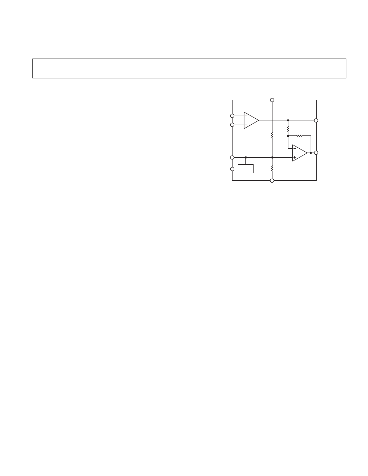
FUNCTIONAL BLOCK DIAGRAM
V
OUT
B
IN –
IN +
SHUTDOWN
BYPASS
V
OUT
A
V– (GND)
BIAS
REV. A
Information furnished by Analog Devices is believed to be accurate and
reliable. However, no responsibility is assumed by Analog Devices for its
use, nor for any infringements of patents or other rights of third parties that
may result from its use. No license is granted by implication or otherwise
under any patent or patent rights of Analog Devices.
a
Low Distortion 1.5 Watt
Audio Power Amplifier
SSM2211
*
One Technology Way, P.O. Box 9106, Norwood. MA 02062-9106, U.S.A.
Tel: 781/329-4700 www.analog.com
Fax: 781/326-8703 © Analog Devices, Inc., 2002
FEATURES
1.5 W Output
1
Differential (BTL
2
) Output
Single-Supply Operation: 2.7 V to 5.5 V
Functions Down to 1.75 V
Wide Bandwidth: 4 MHz
Highly Stable, Phase Margin: >80 Degrees
Low Distortion: 0.2% THD @ 1 W Output
Excellent Power Supply Rejection
APPLICATIONS
Portable Computers
Personal Wireless Communicators
Hands-Free Telephones
Speakerphones
Intercoms
Musical Toys and Speaking Games
GENERAL DESCRIPTION
The SSM2211 is a high-performance audio amplifier that delivers
1 W RMS of low distortion audio power into a bridge-connected
8 Ω speaker load, (or 1.5 W RMS into 4 Ω load). It operates
over a wide temperature range and is specified for single-supply
voltages between 2.7 V and 5.5 V. When operating from batteries,
it will continue to operate down to 1.75 V. This makes the
SSM2211 the best choice for unregulated applications such as toys
and games. Featuring a 4 MHz bandwidth and distortion below
0.2 % THD @ 1 W, superior performance is delivered at higher
power or lower speaker load impedance than competitive units.
The low differential dc output voltage results in negligible losses
in the speaker winding, and makes high value dc blocking ca-
pacitors unnecessary. Battery life is extended by using the
Shutdown mode, which reduces quiescent current drain to
typically 100 nA.
*Protected by U.S. Patent No. 5,519,576
NOTES
1
1.5 W @ 4 Ω, 25°C ambient, <1% THD, 5 V supply, 4 layer PCB.
2
Bridge Tied Load
The SSM2211 is designed to operate over the –20°C to +85°C
temperature range. The SSM2211 is available in SO-8 and
LFCSP (Lead Frame Chip Scale Package) surface mount pack-
ages. The SO-8 features the patented Thermal Coastline lead
frame (see Figure 12). The advanced mechanical packaging of the
SSM2211 ensures lower chip temperature and enhanced per-
formance relative to standard packaging options. DIP samples
are available; you should request a special quotation on produc-
tion quantities. An evaluation board is available upon request of
your local Analog Device sales office.
Applications include personal portable computers, hands-free
telephones and transceivers, talking toys, intercom systems and
other low voltage audio systems requiring 1 W output power.

REV. A
–2–
SSM2211–SPECIFICATIONS
ELECTRICAL CHARACTERISTICS
Parameter Symbol Conditions Min Typ Max Unit
GENERAL CHARACTERISTICS
Differential Output Offset Voltage V
OOS
A
VD
= 2 4 50 mV
Output Impedance Z
OUT
0.1 Ω
SHUTDOWN CONTROL
Input Voltage High V
IH
I
SY
= < 100 µA 3.0 V
Input Voltage Low V
IL
I
SY
= Normal 1.3 V
POWER SUPPLY
Power Supply Rejection Ratio PSRR V
S
= 4.75 V to 5.25 V 66 dB
Supply Current I
SY
V
O1
= V
O2
= 2.5 V 9.5 mA
Supply Current, Shutdown Mode I
SD
Pin 1 = V
DD
, See TPC 29 100 nA
DYNAMIC PERFORMANCE
Gain Bandwidth GBP 4 MHz
Phase Margin Ø
0
86 Degrees
AUDIO PERFORMANCE
Total Harmonic Distortion THD + N P = 0.5 W into 8 Ω, f = 1 kHz 0.15 %
Total Harmonic Distortion THD + N P = 1.0 W into 8 Ω, f = 1 kHz 0.2 %
Voltage Noise Density e
n
f = 1 kHz 85 nV√Hz
ELECTRICAL CHARACTERISTICS
Parameter Symbol Conditions Min Typ Max Unit
GENERAL CHARACTERISTICS
Differential Output Offset Voltage V
OOS
A
VD
= 2 5 50 mV
Output Impedance Z
OUT
0.1 Ω
SHUTDOWN INPUT
Input Voltage High V
IH
I
SY
= < 100 µA 1.7 V
Input Voltage Low V
IL
1V
POWER SUPPLY
Supply Current I
SY
V
O1
= V
O2
= 1.65 V 5.2 mA
Supply Current, Shutdown Mode I
SD
Pin 1 = V
DD
, See TPC 29 100 nA
AUDIO PERFORMANCE
Total Harmonic Distortion THD + N P = 0.35 W into 8 Ω, f = 1 kHz 0.1 %
ELECTRICAL CHARACTERISTICS
Parameter Symbol Conditions Min Typ Max Unit
GENERAL CHARACTERISTICS
Differential Output Offset Voltage V
OOS
A
VD
= 2 5 50 mV
Output Impedance Z
OUT
0.1 Ω
SHUTDOWN CONTROL
Input Voltage High V
IH
I
SY
= < 100 µA 1.5 V
Input Voltage Low V
IL
I
SY
= Normal 0.8 V
POWER SUPPLY
Supply Current I
SY
V
O1
= V
O2
= 1.35 V 4.2 mA
Supply Current, Shutdown Mode I
SD
Pin 1 = V
DD
, See TPC 29 100 nA
AUDIO PERFORMANCE
Total Harmonic Distortion THD + N P = 0.25 W into 8 Ω, f = 1 kHz 0.1 %
Specifications subject to change without notice
(V
S
= 5.0 V, T
A
= 25C, R
L
= 8 , C
B
= 0.1 F, V
CM
= V
D
/2, unless otherwise noted.)
(V
S
= 3.3 V, T
A
= 25C, R
L
= 8 , C
B
= 0.1F, V
CM
= V
D
/2, unless otherwise noted.)
(V
S
= 2.7 V, T
A
= 25C, R
L
= 8 , C
B
= 0.1 F, V
CM
= V
S
/2, unless otherwise noted.)
SSM2211
REV. A
–3–
ABSOLUTE MAXIMUM RATINGS
1, 2
Supply Voltage . . . . . . . . . . . . . . . . . . . . . . . . . . . . . . . . . . . 6 V
Input Voltage . . . . . . . . . . . . . . . . . . . . . . . . . . . . . . . . . . . V
DD
Common Mode Input Voltage . . . . . . . . . . . . . . . . . . . . . . V
DD
ESD Susceptibility . . . . . . . . . . . . . . . . . . . . . . . . . . . . . 2000 V
Storage Temperature Range . . . . . . . . . . . . 65°C to +150°C
Operating Temperature Range . . . . . . . . . . . 20°C to +85°C
Junction Temperature Range . . . . . . . . . . . . 65°C to +165°C
Lead Temperature Range (Soldering, 60 sec) . . . . . . . . 300°C
NOTES
1
Absolute maximum ratings apply at 25°C, unless otherwise noted.
2
Stresses above those listed under Absolute Maximum Ratings may cause perma-
nent damage to the device. This is a stress rating only; the functional operation of
the device at these or any other conditions above those indicated in the operational
sections of this specification is not implied. Exposure to absolute maximum rating
conditions for extended periods may affect device reliability.
Package Type
JA
1
JC
Units
8-Lead LFCSP (CP)
2
50 °C/W
8-Lead SOIC (S) 98 43 °C/W
8-Lead PDIP (P)
3
103 43 °C/W
NOTES
1
For the SOIC package, θ
JA
is measured with the device soldered to a 4-layer
printed circuit board.
2
For the LFCSP package, θ
JA
is measured with exposed lead frame soldered to
the printed circuit board.
3
Special order only.
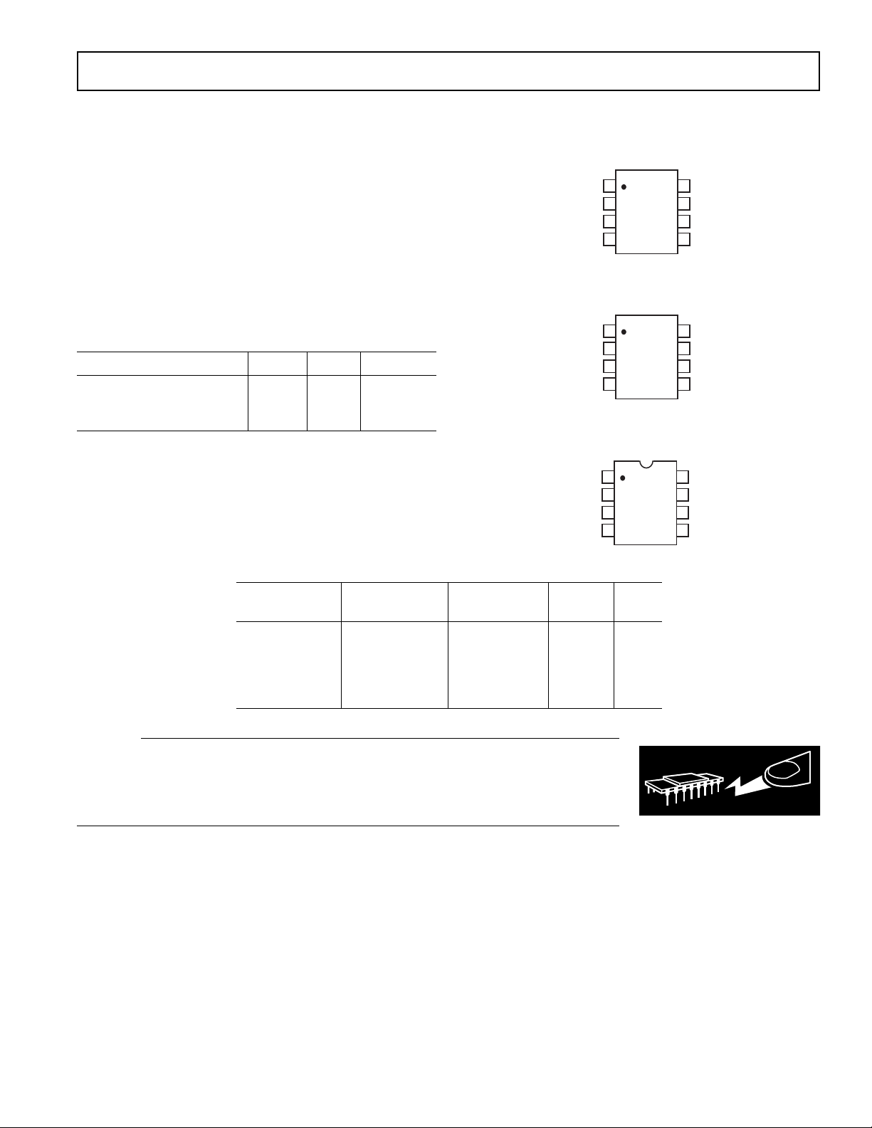
PIN CONFIGURATIONS
8-Lead SOIC
(SO-8)
1
2
3
4
8
7
6
5
TOP VIEW
(Not to Scale)
SHUTDOWN
V
OUT
A
+V
–V
V
OUT
B
BYPASS
+IN
–IN
8-Lead LFCSP
(CP-8)
1
2
3
4
8
7
6
5
TOP VIEW
(Not to Scale)
SHUTDOWN
V
OUT
A
+V
–V
V
OUT
B
BYPASS
+IN
–IN
8-Lead Plastic DIP
(N-8)
1
2
3
4
8
7
6
5
TOP VIEW
(Not to Scale)
SHUTDOWN
V
OUT
A
+V
–V
V
OUT
B
BYPASS
+IN
–IN
CAUTION
ESD (electrostatic discharge) sensitive device. Electrostatic charges as high as 4000 V readily
accumulate on the human body and test equipment and can discharge without detection. Although
the SSM2211 features proprietary ESD protection circuitry, permanent damage may occur on
devices subjected to high energy electrostatic discharges. Therefore, proper ESD precautions are
recommended to avoid performance degradation or loss of functionality.
WARNING!
ESD SENSITIVE DEVICE
ORDERING GUIDE
Temperature Package Package
Model Range Description Options Brand
SSM2211CP-Reel –20°C to +85°C 8-Lead LFCSP CP-8 B5A
SSM2211S –20°C to +85°C 8-Lead SOIC SO-8
SSM2211S-Reel –20°C to +85°C 8-Lead SOIC SO-8
SSM2211S-Reel7 –20°C to +85°C 8-Lead SOIC SO-8
SSM2211P –20°C to +85°C 8-Lead PDIP N-8
*
*Special order only.
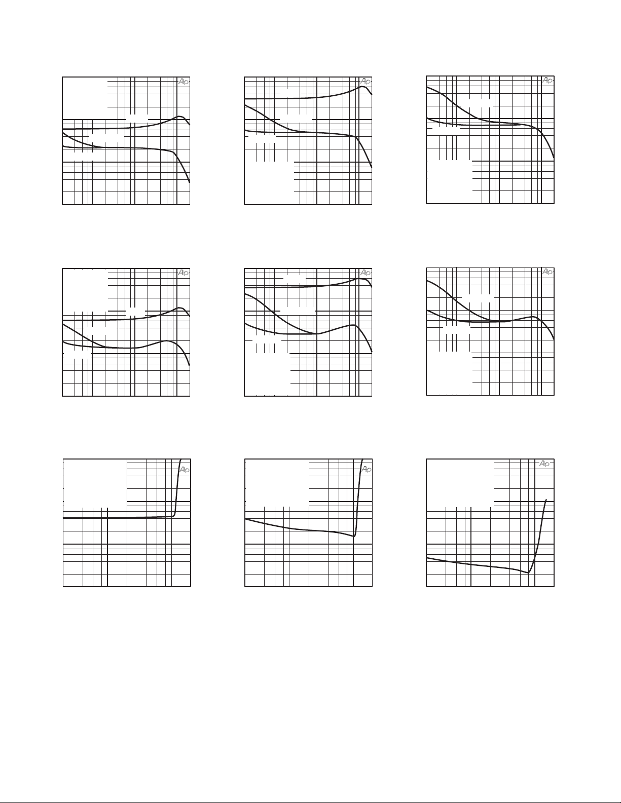
FREQUENCY – Hz
THD + N – %
10
1
0.01
20 100 20k
1k 10k
0.1
C
B
= 0
C
B
= 0.1F
C
B
= 1F
T
A
= 25C
V
DD
= 5V
A
VD
= 2 (BTL)
R
L
= 8
P
L
= 500mW
TPC 1. THD+N vs. Frequency
FREQUENCY – Hz
THD + N – %
10
1
0.01
20 100 20k
1k 10k
0.1
C
B
= 0
C
B
= 0.1F
C
B
= 1F
T
A
= 25C
V
DD
= 5V
A
VD
= 2 (BTL)
R
L
= 8
P
L
= 1W
TPC 4. THD+N vs. Frequency
P
OUTPUT
– W
THD + N – %
10
1
0.01
20n 0.1 2
0.1
1
T
A
= 25C
V
DD
= 5V
A
VD
= 2 (BTL)
R
L
= 8
FREQUENCY = 20Hz
C
B
= 0.1F
TPC 7. THD+N vs. P
OUTPUT
FREQUENCY – Hz
THD + N – %
10
1
0.01
20 100 20k
1k 10k
0.1
C
B
= 0.1F
C
B
= 1F
T
A
= 25C
V
DD
= 5V
A
VD
= 20 (BTL)
R
L
= 8
P
L
= 500mW
TPC 3. THD+N vs. Frequency
FREQUENCY – Hz
THD + N – %
10
1
0.01
20 100 20k
1k 10k
0.1
C
B
= 0.1F
C
B
= 1F
T
A
= 25C
V
DD
= 5V
A
VD
= 20 (BTL)
R
L
= 8
P
L
= 1W
TPC 6. THD+N vs. Frequency
P
OUTPUT
– W
THD + N –%
10
1
0.01
20n 0.1 2
0.1
1
T
A
= 25C
V
DD
= 5V
A
VD
= 2 (BTL)
R
L
= 8
FREQUENCY = 20kHz
C
B
= 0.1F
TPC 9. THD+N vs. P
OUTPUT
FREQUENCY – Hz
THD + N – %
10
1
0.01
20 100 20k
1k 10k
0.1
C
B
= 0
C
B
= 0.1F
C
B
= 1F
T
A
= 25C
V
DD
= 5V
A
VD
= 10 (BTL)
R
L
= 8
P
L
= 500mW
TPC 2. THD+N vs. Frequency
FREQUENCY – Hz
THD + N – %
10
1
0.01
20 100 20k
1k 10k
0.1
C
B
= 0
C
B
= 0.1F
C
B
= 1F
T
A
= 25C
V
DD
= 5V
A
VD
= 10 (BTL)
R
L
= 8
P
L
= 1W
TPC 5
.
THD+N vs. Frequency
P
OUTPUT
– W
THD + N – %
10
1
0.01
20n 0.1 2
0.1
1
T
A
= 25C
V
DD
= 5V
A
VD
= 2 (BTL)
R
L
= 8
FREQUENCY = 1kHz
C
B
= 0.1F
TPC 8. THD+N vs. P
OUTPUT
SSM2211–Typical Performance Characteristics
REV. A
–4–
SSM2211
REV. A
–5–
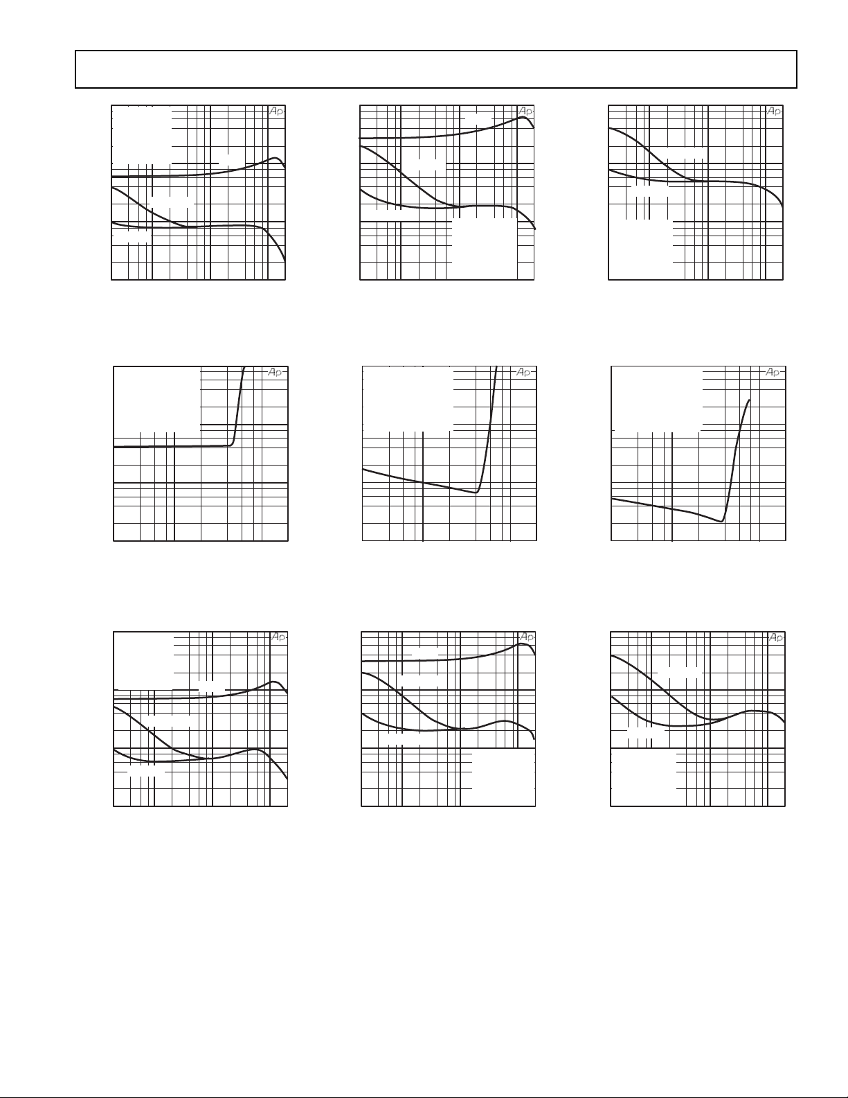
FREQUENCY – Hz
THD + N – %
10
1
0.01
20 100 20k
1k 10k
0.1
C
B
= 0
C
B
= 0.1F
C
B
= 1F
T
A
= 25C
V
DD
= 3.3V
A
VD
= 2 (BTL)
R
L
= 8
P
L
= 350mW
TPC 10. THD+N vs. Frequency
P
OUTPUT
– W
THD + N – %
10
1
0.01
20n 0.1 2
0.1
1
T
A
= 25C
V
DD
= 3.3V
A
VD
= 2 (BTL)
R
L
= 8
FREQUENCY = 20Hz
C
B
= 0.1F
TPC 13. THD+N vs. P
OUTPUT
FREQUENCY – Hz
THD + N – %
10
1
0.01
20 100 20k
1k 10k
0.1
C
B
= 0
C
B
= 0.1F
C
B
= 1F
T
A
= 25C
V
DD
= 2.7V
A
VD
= 2 (BTL)
R
L
= 8
P
L
= 250mW
TPC 16. THD+N vs. Frequency
FREQUENCY – Hz
THD + N – %
10
1
0.01
20 100 20k
1k 10k
0.1
C
B
= 0.1F
C
B
= 1F
T
A
= 25C
V
DD
= 3.3V
A
VD
= 20 (BTL)
R
L
= 8
P
L
= 350mW
TPC 12. THD+N vs. Frequency
P
OUTPUT
– W
THD + N – %
10
1
0.01
20n 0.1 2
0.1
1
T
A
= 25C
V
DD
= 3.3V
A
VD
= 2 (BTL)
R
L
= 8
FREQUENCY = 20kHz
C
B
= 0.1F
TPC 15. THD+N vs. Frequency
FREQUENCY – Hz
THD + N – %
10
1
0.01
20 100 20k
1k 10k
0.1
C
B
= 0.1F
C
B
= 1F
T
A
= 25C
V
DD
= 2.7V
A
VD
= 20 (BTL)
R
L
= 8
P
L
= 250mW
TPC 18. THD+N vs. Frequency
FREQUENCY – Hz
THD + N – %
10
1
0.01
20 100 20k
1k 10k
0.1
C
B
= 0
C
B
= 0.1F
C
B
= 1F
T
A
= 25C
V
DD
= 3.3V
A
VD
= 10 (BTL)
R
L
= 8
P
L
= 350mW
TPC 11. THD+N vs. Frequency
P
OUTPUT
– W
THD + N – %
10
1
0.01
20n 0.1 2
0.1
1
T
A
= 25C
V
DD
= 3.3V
A
VD
= 2 (BTL)
R
L
= 8
FREQUENCY = 1kHz
C
B
= 0.1F
TPC 14. THD+N vs. P
OUTPUT
FREQUENCY – Hz
THD + N – %
10
1
0.01
20 100 20k
1k 10k
0.1
C
B
= 0
C
B
= 0.1F
C
B
= 1F
T
A
= 25C
V
DD
= 2.7V
A
VD
= 10 (BTL)
R
L
= 8
P
L
= 250mW
TPC 17. THD+N vs. Frequency
Loading...