


OP467ARC-883C
Table of contents
 Loading...
Analog Devices OP467ARC-883C, OP467GP, OP467GS, OP467GS-REEL, OP467GBC Datasheet
...
Quad Precision, High-Speed
1
2
3
4
5
6
7
8
OUT A
–IN A
+IN A
V+
+IN B
–IN B
OUT B
16
15
14
13
12
11
10
9
OUT D
–IN D
+IN D
V–
+IN C
–IN C
OUT C
NC
NC
OP467
NC = NO CONNECT
a
FEATURES
High Slew Rate – 170 V/s
Wide Bandwidth – 28 MHz
Fast Settling Time – <200 ns to 0.01%
Low Offset Voltage – <500 V
Unity-Gain Stable
Low Voltage Operation ⴞ5 V to ⴞ15 V
Low Supply Current – <10 mA
Drives Capacitive Loads
APPLICATIONS
High-Speed Image Display Drivers
High Frequency Active Filters
Fast Instrumentation Amplifiers
High-Speed Detectors
Integrators
Photo Diode Preamps
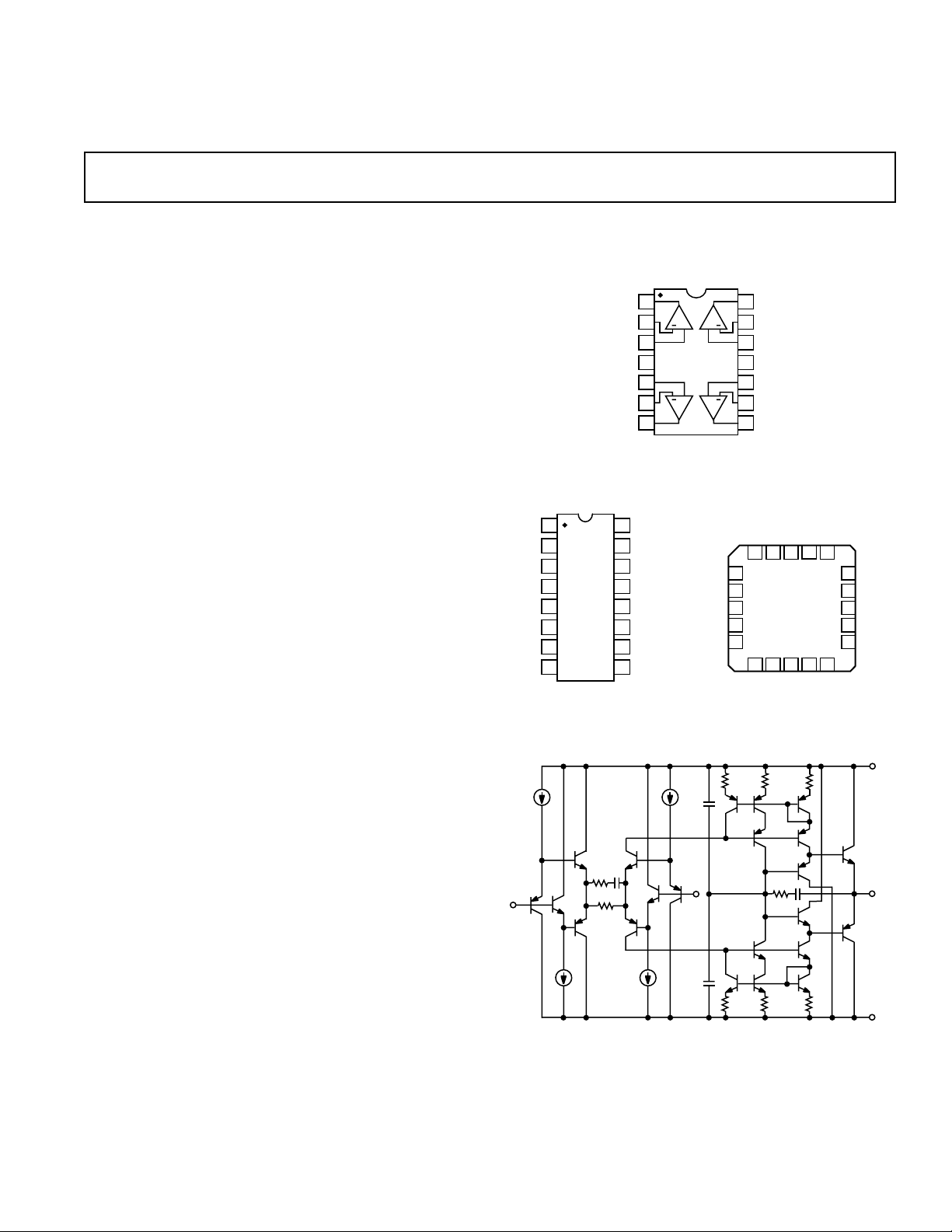
GENERAL DESCRIPTION
The OP467 is a quad, high-speed, precision operational amplifier. It offers the performance of a high-speed op amp combined
with the advantages of a precision operational amplifier all in a
single package. The OP467 is an ideal choice for applications
where, traditionally, more than one op amp was used to achieve
this level of speed and precision.
The OP467’s internal compensation ensures stable unity-gain
operation, and it can drive large capacitive loads without oscillation. With a gain bandwidth product of 28 MHz driving a 30 pF
load, output slew rate in excess of 170 V/µs, and settling time
to 0.01% in less than 200 ns, the OP467 provides excellent
dynamic accuracy in high-speed data-acquisition systems. The
channel-to-channel separation is typically 60 dB at 10 MHz.
The dc performance of OP467 includes less than 0.5 mV of
offset, voltage noise density below 6 nV/√Hz and total supply
current under 10 mA. Common-mode rejection and power
supply rejection ratios are typically 85 dB. PSRR is maintained
to better than 40 dB with input frequencies as high as 1 MHz.
The low offset and drift plus high speed and low noise, make the
OP467 usable in applications such as high-speed detectors and
instrumentation.
The OP467 is specified for operation from ±5 V to ±15 V over
the extended industrial temperature range (–40°C to +85°C) and
is available in 14-lead plastic and ceramic DIP, plus 16-lead
SOIC and 20-terminal LCC surface mount packages.
Contact your local sales office for MIL-STD-883 data sheet
and availability.
16-Lead SOIC
(S Suffix)
–IN
Operational Amplifier
OP467
PIN CONNECTIONS
14-Lead Ceramic DIP (Y Suffix) and
14-Lead Plastic DIP (P Suffix)
OUT A
–IN A
+IN A
+IN B
–IN B
OUT B
1
2
+ +
3
4
V+
OP467
5
++
6
7
+IN
14
OUT D
13
–IN D
+IN D
12
11
V–
10
+IN C
9
–IN C
8
OUT C
20-Terminal LCC
(RC Suffix)
–IN A
3
+IN A
4
NC
5
V+
NC
+IN B
OP467
6
(TOP VIEW)
7
8
9
10 11
–IN B
NC = NO CONNECT
OUT A
OUT B
NC
NC
OUT D
2012
12 13
OUT C
–IN D
19
+IN D
18
NC
17
16
V–
NC
15
14
+IN C
–IN C
V+
OUT
V–
REV. D
Information furnished by Analog Devices is believed to be accurate and
reliable. However, no responsibility is assumed by Analog Devices for its
use, nor for any infringements of patents or other rights of third parties
which may result from its use. No license is granted by implication or
otherwise under any patent or patent rights of Analog Devices.
Figure 1. Simplified Schematic
One Technology Way, P.O. Box 9106, Norwood, MA 02062-9106, U.S.A.
Tel: 781/329-4700 World Wide Web Site: www.analog.com
Fax: 781/326-8703 © Analog Devices, Inc., 2001

OP467–SPECIFICATIONS
ELECTRICAL CHARACTERISTICS
(@ VS = ⴞ15.0 V, TA = 25ⴗC unless otherwise noted.)
Parameter Symbol Conditions Min Typ Max Unit
INPUT CHARACTERISTICS
Offset Voltage V
Input Bias Current I
Input Offset Current I
OS
B
OS
Common-Mode Rejection CMR V
CMR V
Large Signal Voltage Gain A
Offset Voltage Drift ∆V
Bias Current Drift ∆I
VO
/∆T 3.5 µV/°C
OS
/∆T 0.2 pA/°C
B
–40°C ≤ T
≤ +85°C1mV
A
VCM = 0 V 150 600 nA
= 0 V, –40°C ≤ TA ≤ +85°C 150 700 nA
V
CM
VCM = 0 V 10 100 nA
V
= 0 V, –40°C ≤ TA ≤ +85°C 10 150 nA
CM
= ±12 V 80 90 dB
CM
= ±12 V, –40°C ≤ TA ≤ +85°C8088 dB
CM
RL = 2 kΩ 83 86 dB
= 2 kΩ, –40°C ≤ TA ≤ +85°C77.5 dB
R
L
0.2 0.5 mV
Long Term Offset Voltage Drift ∆VOS/∆T Note 1 750 µV
OUTPUT CHARACTERISTICS
Output Voltage Swing V
O
RL = 2 kΩ±13.0 ±13.5 V
RL = 2 kΩ, –40°C ≤ TA ≤ +85°C ±12.9 ± 13.12 V
POWER SUPPLY
2
Power Supply Rejection Ratio PSRR ± 4.5 V ≤ VS = ±18 V 96 120 dB
Supply Current I
Supply Voltage Range V
SY
–40°C ≤ T
VO = 0 V 8 10 mA
V
= 0 V, –40°C ≤ TA ≤ +85°C13mA
O
S
≤ +85°C 86 115 dB
A
±4.5 ± 18 V
DYNAMIC PERFORMANCE
Gain Bandwidth Product GBP AV = +1, CL = 30 pF 28 MHz
Slew Rate SR V
Full-Power Bandwidth BW
Settling Time t
Phase Margin θ
ρ
S
0
= 10 V Step, RL = 2 kΩ, CL = 30 pF
IN
A
= +1 125 170 V/µs
V
A
= –1 350 V/µs
V
VIN = 10 V Step 2.7 MHz
To 0.01%, VIN = 10 V Step 200 ns
45 Degrees
Input Capacitance
Common Mode 2.0 pF
Differential 1.0 pF
NOISE PERFORMANCE
Voltage Noise e
Voltage Noise Density e
Current Noise Density i
NOTES
1
Long-Term Offset Voltage Drift is guaranteed by 1000 hrs. Life test performed on three independent wafer lots at 125 °C, with an LTPD of 1.3.
2
For proper operation the positive supply must be sequenced ON before the negative supply.
Specifications subject to change without notice.
p-p f = 0.1 Hz to 10 Hz 0.15 µV p-p
N
N
N
f = 1 kHz 6 nV/√Hz
f = 1 kHz 8 pA/√Hz
–2–
REV. D

OP467
ELECTRICAL CHARACTERISTICS
(@ VS = ⴞ5.0 V, TA = 25ⴗC unless otherwise noted.)
Parameter Symbol Conditions Min Typ Max Unit
INPUT CHARACTERISTICS
Offset Voltage V
Input Bias Current I
Input Offset Current I
OS
B
OS
Common-Mode Rejection CMR V
CMR V
Large Signal Voltage Gain A
Offset Voltage Drift ∆V
VO
/∆T3 5µV/°C
OS
–40°C ≤ T
≤ +85°C1mV
A
VCM = 0 V 125 600 nA
V
= 0 V, –40°C ≤ TA ≤ +85°C 150 700 nA
CM
VCM = 0 V 20 100 nA
= 0 V, –40°C ≤ TA ≤ +85°C 150 nA
V
CM
= ±2.0 V 76 85 dB
CM
= ±2.0 V, –40°C ≤ TA ≤ +85°C76 80 dB
CM
RL = 2 kΩ 80 83 dB
R
= 2 kΩ, –40°C ≤ TA ≤ +85°C74 dB
L
0.3 0.5 mV
Bias Current Drift ∆IB/∆T 0.2 pA/°C
OUTPUT CHARACTERISTICS
Output Voltage Swing V
O
RL = 2 kΩ±3.0 ± 3.5 V
RL = 2 kΩ, –40°C ≤ TA ≤ +85°C ±3.0 ± 3.20 V
POWER SUPPLY
Power Supply Rejection Ratio PSRR ±4.5 V ≤ VS = ±5.5 V 92 107 dB
≤ +85°C 83 105 dB
A
Supply Current I
SY
–40°C ≤ T
VO = 0 V 8 10 mA
VO = 0 V, –40°C ≤ TA ≤ +85°C12mA
DYNAMIC PERFORMANCE
Gain Bandwidth Product GBP AV = +1 22 MHz
Slew Rate SR V
Full-Power Bandwidth BW
Settling Time t
Phase Margin θ
ρ
S
0
= 5 V Step, RL = 2 kΩ, CL = 39 pF
IN
A
= +1 90 V/µs
V
A
= –1 90 V/µs
V
VIN = 5 V Step 2.5 MHz
To 0.01%, VIN = 5 V Step 280 ns
45 Degrees
NOISE PERFORMANCE
Voltage Noise eN p-p f = 0.1 Hz to 10 Hz 0.15 µV p-p
Voltage Noise Density e
Current Noise Density i
Specifications subject to change without notice.
N
N
f = 1 kHz 7 nV/√Hz
f = 1 kHz 8 pA/√Hz
REV. D
–3–
OP467
WAFER TEST LIMITS
1
(@ VS = ⴞ15.0 V, TA = 25ⴗC unless otherwise noted.)
Parameter Symbol Conditions Limit Unit
Offset Voltage V
Input Bias Current I
Input Offset Current I
Input Voltage Range
2
OS
B
OS
Common-Mode Rejection Ratio CMRR V
VCM = 0 V 600 nA max
VCM = 0 V 100 nA max
= ±12 V 80 dB min
CM
±0.5 mV max
±12 V min/max
Power Supply Rejection Ratio PSRR V = ±4.5 V to ±18 V 96 dB min
Large Signal Voltage Gain A
Output Voltage Range V
Supply Current I
NOTES
1
Electrical tests and wafer probe to the limits shown. Due to variations in assembly methods and normal yield loss, yield after packaging is not guaranteed for standard
product dice. Consult factory to negotiate specifications based on dice lot qualifications through sample lot assembly and testing.
2
Guaranteed by CMR test.
ABSOLUTE MAXIMUM RATINGS
Supply Voltage2 . . . . . . . . . . . . . . . . . . . . . . . . . . . . . . ±18 V
Input Voltage
Differential Input Voltage
3
. . . . . . . . . . . . . . . . . . . . . . . . . . . . . . . . ±18 V
3
. . . . . . . . . . . . . . . . . . . . . . ±26 V
1
VO
O
SY
Output Short-Circuit Duration . . . . . . . . . . . . . . . . . . Limited
Storage Temperature Range
Y, RC Packages . . . . . . . . . . . . . . . . . . . . –65°C to +175°C
P, S Packages . . . . . . . . . . . . . . . . . . . . . . –65°C to +150°C
Operating Temperature Range
OP467A . . . . . . . . . . . . . . . . . . . . . . . . . . –55°C to +125°C
RL = 2 kΩ 83 dB min
RL = 2 kΩ±13.0 V min
VO = 0 V, RL = ∞ 10 mA max
ORDERING GUIDE
Temperature Package Package
Model Ranges Descriptions Options
OP467ARC/883C –55°C to +125°C 20-Terminal LCC E-20A
OP467AY/883C –55°C to +125°C 14-Lead Cerdip Q-14
OP467GBC DIE
OP467GP –40°C to +85°C 14-Lead Plastic DIP N-14
OP467GS –40°C to +85°C 16-Lead SOIC R-16
OP467GS-REEL –40°C to +85°C 16-Lead SOIC R-16
OP467G . . . . . . . . . . . . . . . . . . . . . . . . . . . –40°C to +85°C
Junction Temperature Range
Y, RC Packages . . . . . . . . . . . . . . . . . . . . –65°C to +175°C
DICE CHARACTERISTICS
P, S Packages . . . . . . . . . . . . . . . . . . . . . . –65°C to +150°C
Lead Temperature Range (Soldering, 60 sec) . . . . . . . . 300°C
Package Type
4
A
JC
Unit
14-Lead Cerdip (Y) 94 10 °C/W
14-Lead Plastic DIP (P) 76 33 °C/W
16-Lead SOIC (S) 88 23 °C/W
20-Terminal LCC (RC) 78 33 °C/W
NOTES
1
Absolute maximum ratings apply to both DICE and packaged parts, unless
otherwise noted.
2
For proper operation the positive supply must be sequenced ON before the
negative supply.
3
For supply voltages less than ± 18 V, the absolute maximum input voltage is equal
to the supply voltage.
4
θJA is specified for the worst-case conditions, i.e., θJA is specified for device in socket
for cerdip, P-DIP, and LCC packages; θJA is specified for device soldered in circuit
board for SOIC package.
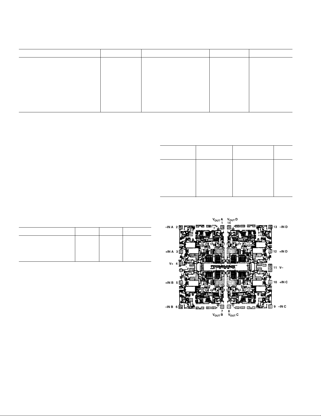
OP467 Die Size 0.111 ⫻ 0.100 inch, 11,100 sq. mils Substrate is Connected to V+, Number of Transistors 165
–4–
REV. D
Typical Performance Characteristics–
OP467
80
70
60
50
40
30
20
10
OPEN-LOOP GAIN – dB
0
–10
–20
1k 10k 100M10M1M100k
GAIN
PHASE
FREQUENCY – Hz
TPC 1. Open-Loop Gain, Phase vs. Frequency
80
60
40
20
CLOSED-LOOP GAIN – dB
0
VS = ⴞ15V
R
= 1M⍀
L
= 30pF
C
L
VS = ⴞ15V
= 25ⴗC
T
A
0
90
180
PHASE SHIFT – Degrees
100
VS = ⴞ15V
= 25ⴗC
T
A
80
60
A
= +100
VCL
40
IMPEDANCE – ⍀
20
0
1k 100k10k100
FREQUENCY – Hz
A
= +10
VCL
A
= +1
VCL
1M
TPC 4. Closed-Loop Output Impedance vs. Frequency
0.3
GAIN ERROR – dB
0.2
0.1
0.0
–0.1
–0.2
–0.3
VS = ⴞ5V
VS = ⴞ15V
–20
100k 100M10M1M10k
FREQUENCY – Hz
TPC 2. Closed-Loop Gain vs. Frequency
25
20
15
TA = +125ⴗC
T
= +25ⴗC
A
10
= –55ⴗC
T
OPEN-LOOP GAIN – V/mV
A
5
0
0
ⴞ5
SUPPLY VOLTAGE – Volts
TPC 3. Open-Loop Gain vs. Supply Voltage
5.8
100k 1M 10M
FREQUENCY – Hz
3.4
TPC 5. Gain Linearity vs. Frequency
30
25
20
15
ⴞ15ⴞ10
ⴞ20
10
VS = ⴞ15V
MAXIMUM OUTPUT SWING – Volts
= 25ⴗC
T
5
A
= 2k⍀
R
L
0
TPC 6. Max V
10k 10M1M100k1k
FREQUENCY – Hz
Swing vs. Frequency
OUT
A
VCL
= +1
A
= –1
VCL
REV. D
–5–
Loading...