


a
Balanced Line Driver
SSM2142
FEATURES
Transformer-Like Balanced Output
Drives 10 V RMS Into a 600 V Load
Stable When Driving Large Capacitive Loads and Long
Cables
Low Distortion
0.006% typ 20 Hz–20 kHz, 10 V RMS into 600 V
High Slew Rate
15 V/ms typ
Low Gain Error
(Differential or Single-Ended); 0.7% typ
Outputs Short-Circuit Protected
Available In Space-Saving 8-Pin Mini-DIP Package
Low Cost
APPLICATIONS
Audio Mix Consoles
Distribution Amplifiers
Graphic and Parametric Equalizers
Dynamic Range Processors
Digital Effects Processors
Telecommunications Systems
Industrial Instrumentation
Hi-Fi Equipment
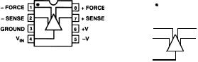
FUNCTIONAL BLOCK DIAGRAM
VIN
|
50Ω |
|
+OUT FORCE |
|
+OUT SENSE |
|
10kΩ |
|
– OUT SENSE |
|
50Ω |
|
– OUT FORCE |
ALL RESISTORS 30kΩ |
10kΩ |
UNLESS OTHERWISE |
|
INDICATED |
|
GND |
|
GENERAL DESCRIPTION
The SSM2142 is an integrated differential-output buffer amplifier that converts a single-ended input signal to a balanced output signal pair with high output drive. By utilizing low noise thermally matched thin film resistors and high slew rate amplifiers, the SSM2142 helps maintain the sonic quality of audio systems by eliminating power line hum, RF interference, voltage drops, and other externally generated noise commonly encountered with long audio cable runs. Excellent rejection of common-mode noise and offset errors is achieved by laser trimming of the onboard resistors, assuring high gain accuracy. The carefully designed output stage of the SSM2142 is capable of driving difficult loads, yielding low distortion performance despite extremely long cables or loads as low as 600 Ω, and is stable over a wide range of operating conditions.
Based on a cross-coupled, electronically balanced topology, the SSM2142 mimics the performance of fully balanced transformer-based solutions for line driving. However, the SSM2142 maintains lower distortion and occupies much less board space than transformers while achieving comparable common-mode rejection performance with reduced parts count.
The SSM2142 in tandem with the SSM2141 differential receiver establishes a complete, reliable solution for driving and receiving audio signals over long cables. The SSM2141 features an Input Common-Mode Rejection Ratio of 100 dB at 60 Hz. Specifications demonstrating the performance of this typical system are included in the data sheet.
REV. B
Information furnished by Analog Devices is believed to be accurate and reliable. However, no responsibility is assumed by Analog Devices for its use, nor for any infringements of patents or other rights of third parties which may result from its use. No license is granted by implication or otherwise under any patent or patent rights of Analog Devices.
One Technology Way, P.O. Box 9106, Norwood, MA 02062-9106, U.S.A. Tel: 617/329-4700 Fax: 617/326-8703
|
(VS = 618 V, –408C ≤ TA ≤ +858C, operating in differential mode unless otherwise |
|||||
SSM2142–SPECIFICATIONS noted. Typical characteristics apply to operation at TA = +258C.) |
|
|||||
Parameter |
Symbol |
Conditions |
Min |
Typ |
Max |
Units |
|
|
|
|
|
|
|
INPUT IMPEDANCE |
ZIN |
|
|
10 |
|
kΩ |
INPUT CURRENT |
IIN |
VIN = ±7.071 V |
|
±750 |
±900 |
μA |
GAIN, DIFFERENTIAL |
|
|
5.8 |
5.98 |
|
dB |
|
|
|
|
|
|
|
GAIN, SINGLE-ENDED |
|
Single-Ended Mode |
5.7 |
5.94 |
|
dB |
|
|
|
|
|
|
|
GAIN ERROR, DIFFERENTIAL |
|
RL = 600 Ω |
|
0.7 |
2 |
% |
POWER SUPPLY REJECTION |
|
VS = ±13 V to ±18 V |
|
|
|
|
RATIO STATIC |
PSRR |
60 |
80 |
|
dB |
|
|
|
|
|
|
|
|
OUTPUT COMMON-MODE REJECTION |
OCMR |
See Test Circuit; f = 1 kHz |
–38 |
–45 |
|
dB |
|
|
|
|
|
|
|
OUTPUT SIGNAL BALANCE RATIO |
SBR |
See Test Circuit; f = 1 kHz |
–35 |
–40 |
|
dB |
|
|
|
|
|
|
|
TOTAL HARMONIC DISTORTION |
|
|
|
|
|
|
Plus Noise |
THD+N |
20 Hz to 20 kHz, |
|
0.006 |
|
% |
|
|
VO = 10 V rms, RL = 600 Ω |
|
|
|
|
SIGNAL-TO-NOISE RATIO |
SNR |
VIN = 0 V |
|
–93.4 |
|
dBu |
HEADROOM |
HR |
CLIP Level = 10.5 V rms |
|
+93.4 |
|
dBu |
|
|
|
|
|
|
|
SLEW RATE |
SR |
|
|
15 |
|
V/μs |
OUTPUT COMMON-MODE |
|
RL = 600 Ω |
|
|
|
|
VOLTAGE OFFSET1 |
VOOS |
–250 |
25 |
250 |
mV |
|
DIFFERENTIAL OUTPUT |
|
RL = 600 Ω |
|
|
|
|
VOLTAGE OFFSET |
VOOD |
–50 |
15 |
50 |
mV |
|
DIFFERENTIAL OUTPUT |
|
VIN = ±7.071 V |
±13.8 |
±14.14 |
|
|
VOLTAGE SWING |
|
|
V |
|||
|
|
|
|
|
|
|
OUTPUT IMPEDANCE |
ZO |
|
45 |
50 |
55 |
Ω |
SUPPLY CURRENT |
ISY |
Unloaded, VIN = 0 V |
|
5.5 |
7.0 |
mA |
OUTPUT CURRENT, SHORT CIRCUIT |
ISC |
|
60 |
70 |
|
mA |
NOTES
1Output common-mode offset voltage can be removed by inserting dc blocking capacitors in the sense lines. See Applications Information.
Specifications subject to change without notice.
ABSOLUTE MAXIMUM RATINGS*
Supply Voltage . . . . . . . . . . . . . . . . . . . . . . . . . . . . . . . . ±18 V Storage Temperature . . . . . . . . . . . . . . . . . . –60°C to +150°C Lead Temperature (Soldering, 60 sec) . . . . . . . . . . . . +300°C Junction Temperature . . . . . . . . . . . . . . . . . . . . . . . . +150°C Operating Temperature Range . . . . . . . . . . . . –40°C to +85°C Output Short Circuit Duration (Both Outputs) . . . . Indefinite
*Stresses above those listed under “Absolute Maximum Ratings” may cause permanent damage to the device. These are stress ratings only; the functional operation of the device at these or any other conditions above those indicated in the operational sections of this specification is not implied. Exposure to absolute maximum rating conditions for extended periods may affect device reliability.
ORDERING GUIDE
|
Operating |
Package |
Package |
Model |
Temperature Range |
Description |
Option |
|
|
|
|
SSM2142P |
–40°C to +85°C |
Plastic DIP |
N-8 |
SSM2142S* |
–40°C to +85°C |
SOL |
R-16 |
PIN CONNECTIONS |
|
|
|
|||
8-Pin Plastic DIP |
16-Pin Wide Body SOL |
|||||
(P Suffix) |
|
|
|
(S Suffix) |
|
|
|
|
|
|
|
|
NC |
|
NC |
1 |
|
|
16 |
|
|
|
|
|
|
|
NC |
|
NC |
2 |
|
|
15 |
|
|
|
|
|
|
|
+ FORCE |
|
– FORCE |
3 |
|
|
14 |
|
|
|
|
|
|
|
+ SENSE |
|
– SENSE |
4 |
|
|
13 |
|
|
|
|
|
|
|
+V |
|
GROUND |
5 |
|
|
12 |
|
|
VIN |
|
|
|
|
–V |
|
6 |
|
|
11 |
||
|
|
|
|
|
|
|
|
NC |
7 |
|
|
10 |
NC |
|
|
|
|
|
|
|
|
NC |
8 |
|
|
9 |
NC |
|
|
|
|
|
|
|
*For availability of SOIC package, contact your local sales office.
–2– |
REV. B |
 Loading...